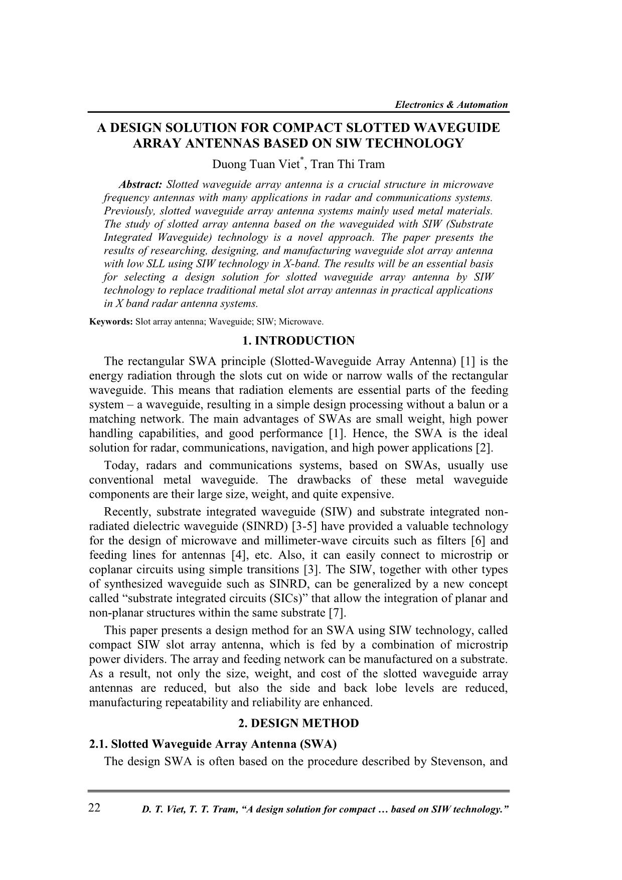
A design solution for compact slotted waveguide array antennas based on SIW technology
Slotted waveguide array antenna is a crucial structure in microwave
frequency antennas with many applications in radar and communications systems.
Previously, slotted waveguide array antenna systems mainly used metal materials.
The study of slotted array antenna based on the waveguided with SIW (Substrate
Integrated Waveguide) technology is a novel approach. The paper presents the
results of researching, designing, and manufacturing waveguide slot array antenna
with low SLL using SIW technology in X-band. The results will be an essential basis
for selecting a design solution for slotted waveguide array antenna by SIW
technology to replace traditional metal slot array antennas in practical applications
in X band radar antenna systems.
Trang 1
Trang 2
Trang 3
Trang 4
Trang 5
Trang 6
Trang 7
Trang 8
Tóm tắt nội dung tài liệu: A design solution for compact slotted waveguide array antennas based on SIW technology
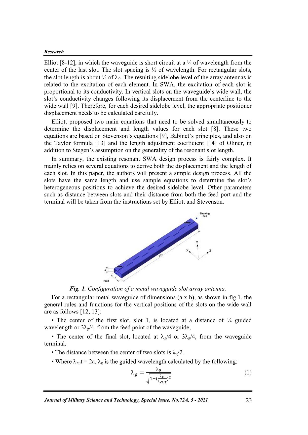
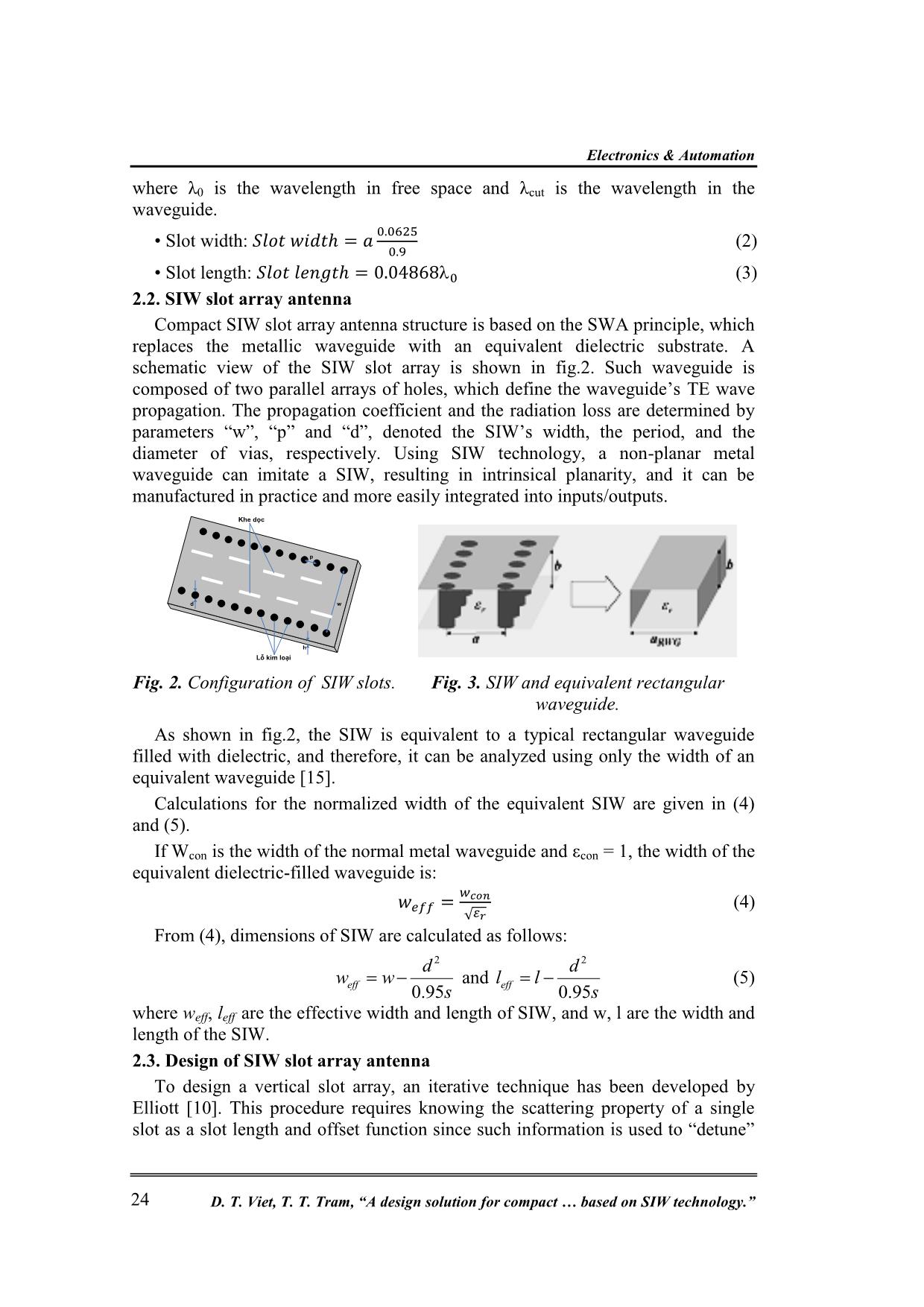
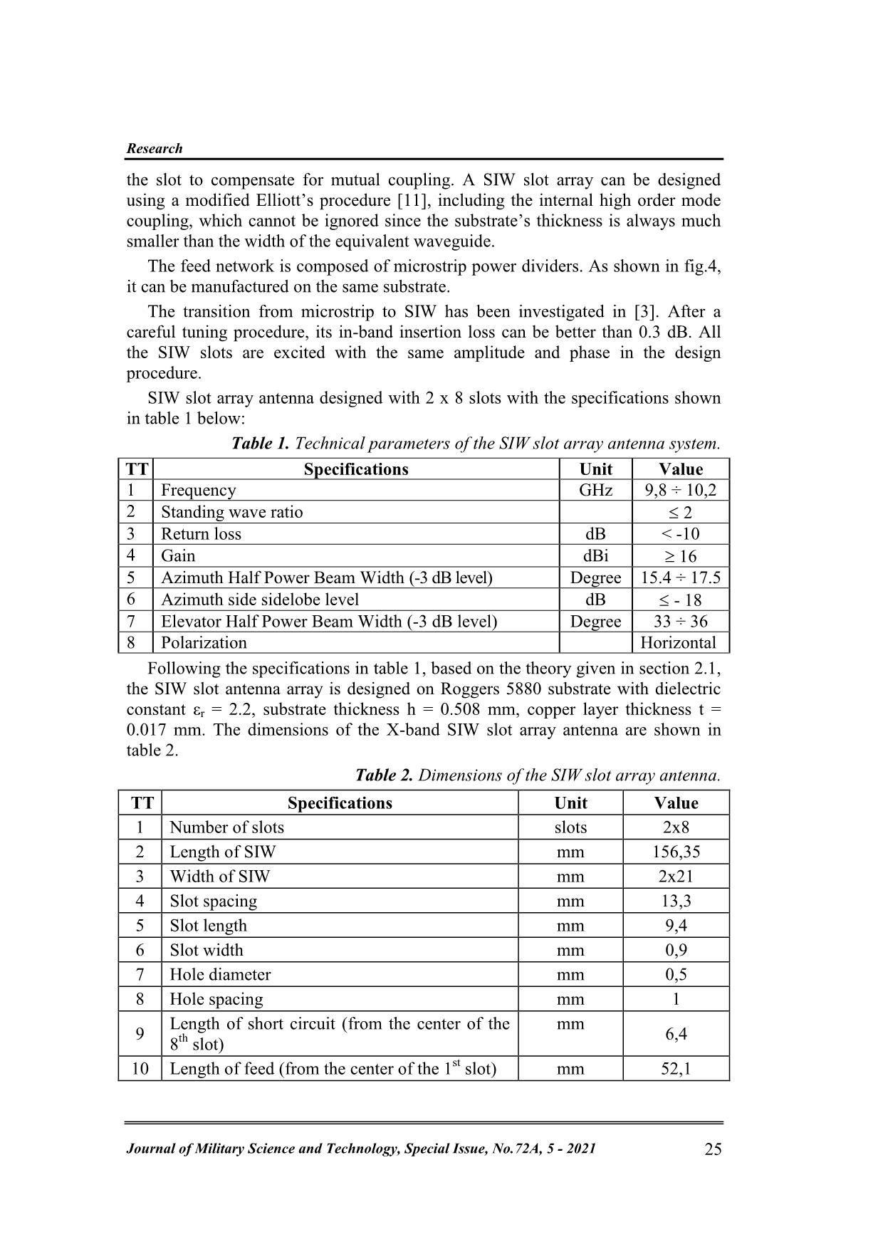
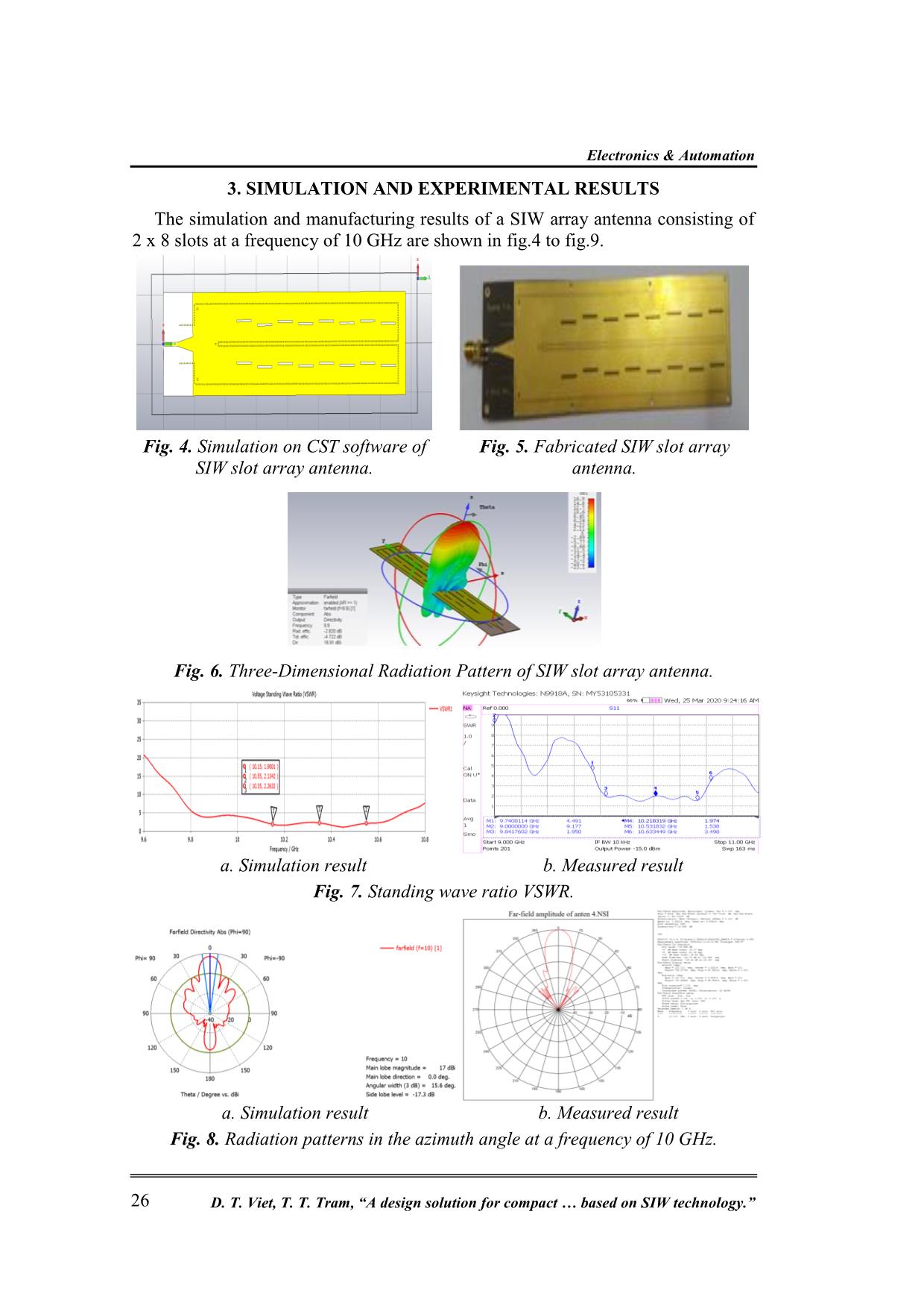
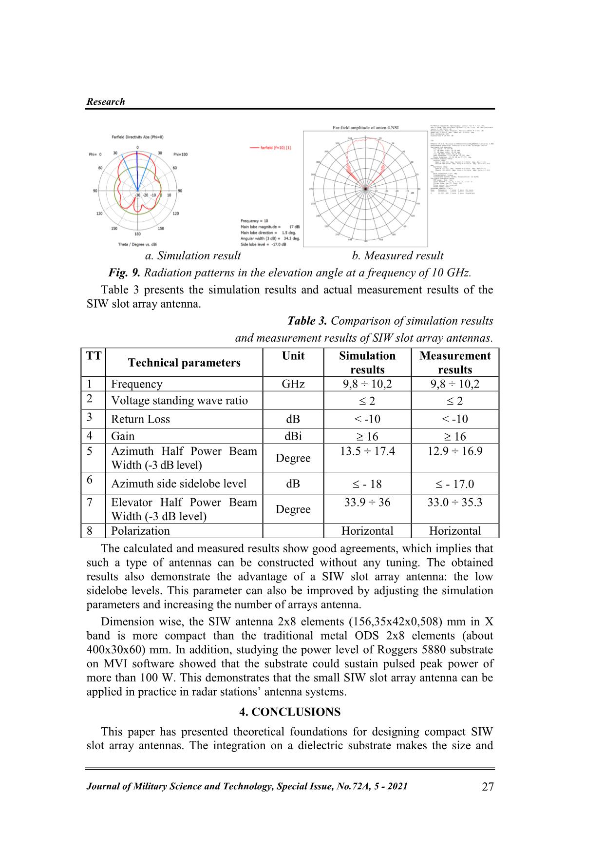
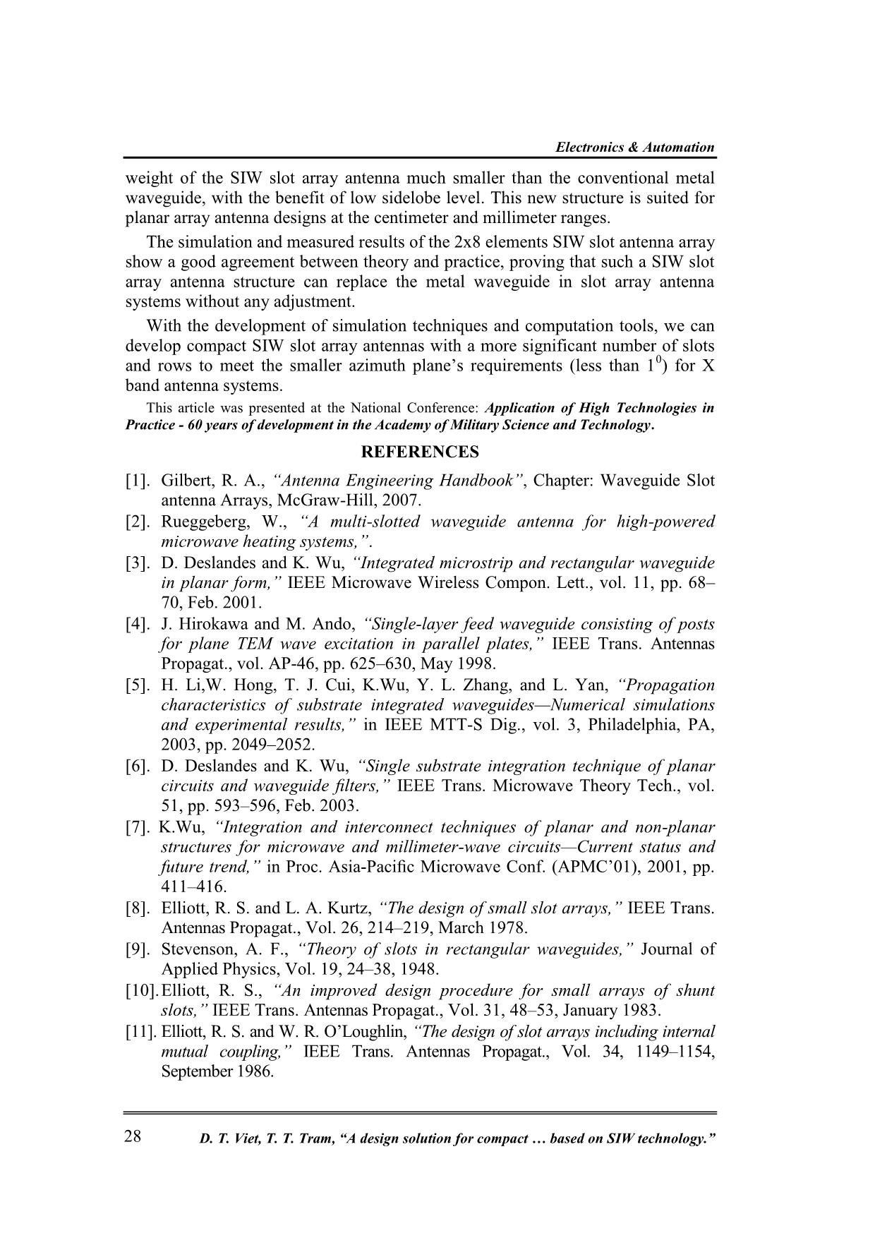
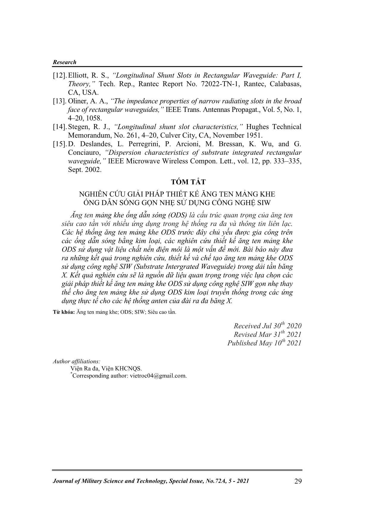
[3]. The SIW, together with other types of synthesized waveguide such as SINRD, can be generalized by a new concept called “substrate integrated circuits (SICs)” that allow the integration of planar and non-planar structures within the same substrate [7]. This paper presents a design method for an SWA using SIW technology, called compact SIW slot array antenna, which is fed by a combination of microstrip power dividers. The array and feeding network can be manufactured on a substrate. As a result, not only the size, weight, and cost of the slotted waveguide array antennas are reduced, but also the side and back lobe levels are reduced, manufacturing repeatability and reliability are enhanced. 2. DESIGN METHOD 2.1. Slotted Waveguide Array Antenna (SWA) The design SWA is often based on the procedure described by Stevenson, and 22 D. T. Viet, T. T. Tram, “A design solution for compact based on SIW technology.” Research Elliot [8-12], in which the waveguide is short circuit at a ¼ of wavelength from the center of the last slot. The slot spacing is ½ of wavelength. For rectangular slots, the slot length is about ¼ of 0. The resulting sidelobe level of the array antennas is related to the excitation of each element. In SWA, the excitation of each slot is proportional to its conductivity. In vertical slots on the waveguide’s wide wall, the slot’s conductivity changes following its displacement from the centerline to the wide wall [9]. Therefore, for each desired sidelobe level, the appropriate positioner displacement needs to be calculated carefully. Elliott proposed two main equations that need to be solved simultaneously to determine the displacement and length values for each slot [8]. These two equations are based on Stevenson’s equations [9], Babinet’s principles, and also on the Taylor formula [13] and the length adjustment coefficient [14] of Oliner, in addition to Stegen’s assumption on the generality of the resonant slot length. In summary, the existing resonant SWA design process is fairly complex. It mainly relies on several equations to derive both the displacement and the length of each slot. In this paper, the authors will present a simple design process. All the slots have the same length and use sample equations to determine the slot’s heterogeneous positions to achieve the desired sidelobe level. Other parameters such as distance between slots and their distance from both the feed port and the terminal will be taken from the instructions set by Elliott and Stevenson. Fig. 1. Configuration of a metal waveguide slot array antenna. For a rectangular metal waveguide of dimensions (a x b), as shown in fig.1, the general rules and functions for the vertical positions of the slots on the wide wall are as follows [12, 13]: • The center of the first slot, slot 1, is located at a distance of ¼ guided wavelength or 3λg/4, from the feed point of the waveguide, • The center of the final slot, located at g/4 or 3λg/4, from the waveguide terminal. • The distance between the center of two slots is λg/2. • Where cut = 2a, λg is the guided wavelength calculated by the following: (1) √ Journal of Military Science and Technology, Special Issue, No.72A, 5 - 2021 23 Electronics & Automation where λ0 is the wavelength in free space and λcut is the wavelength in the waveguide. • Slot width: (2) • Slot length: (3) 2.2. SIW slot array antenna Compact SIW slot array antenna structure is based on the SWA principle, which replaces the metallic waveguide with an equivalent dielectric substrate. A schematic view of the SIW slot array is shown in fig.2. Such waveguide is composed of two parallel arrays of holes, which define the waveguide’s TE wave propagation. The propagation coefficient and the radiation loss are determined by parameters “w”, “p” and “d”, denoted the SIW’s width, the period, and the diameter of vias, respectively. Using SIW technology, a non-planar metal waveguide can imitate a SIW, resulting in intrinsical planarity, and it can be manufactured in practice and more easily integrated into inputs/outputs. Khe dọc p d w h Lỗ kim loại Fig. 2. Configuration of SIW slots. Fig. 3. SIW and equivalent rectangular waveguide. As shown in fig.2, the SIW is equivalent to a typical rectangular waveguide filled with dielectric, and therefore, it can be analyzed using only the width of an equivalent waveguide [15]. Calculations for the normalized width of the equivalent SIW are given in (4) and (5). If Wcon is the width of the normal metal waveguide and εcon = 1, the width of the equivalent dielectric-filled waveguide is: (4) √ From (4), dimensions of SIW are calculated as follows: d 2 d 2 ww and ll (5) eff 0.95s eff 0.95s where weff, leff are the effective width and length of SIW, and w, l are the width and length of the SIW. 2.3. Design of SIW slot array antenna To design a vertical slot array, an iterative technique has been developed by Elliott [10]. This procedure requires knowing the scattering property of a single slot as a slot length and offset function since such information is used to “detune” 24 D. T. Viet, T. T. Tram, “A design solution for compact based on SIW technology.” Research the slot to compensate for mutual coupling. A SIW slot array can be designed using a modified Elliott’s procedure [11], including the internal high order mode coupling, which cannot be ignored since the substrate’s thickness is always much smaller than the width of the equivalent waveguide. The feed network is composed of microstrip power dividers. As shown in fig.4, it can be manufactured on the same substrate. The transition from microstrip to SIW has been investigated in [3]. After a careful tuning procedure, its in-band insertion loss can be better than 0.3 dB. All the SIW slots are excited with the same amplitude and phase in the design procedure. SIW slot array antenna designed with 2 x 8 slots with the specifications shown in table 1 below: Table 1. Technical parameters of the SIW slot array antenna system. TT Specifications Unit Value 1 Frequency GHz 9,8 ÷ 10,2 2 Standing wave ratio 2 3 Return loss dB < -10 4 Gain dBi 16 5 Azimuth Half Power Beam Width (-3 dB level) Degree 15.4 ÷ 17.5 6 Azimuth side sidelobe level dB - 18 7 Elevator Half Power Beam Width (-3 dB level) Degree 33 ÷ 36 8 Polarization Horizontal Following the specifications in table 1, based on the theory given in section 2.1, the SIW slot antenna array is designed on Roggers 5880 substrate with dielectric constant εr = 2.2, substrate thickness h = 0.508 mm, copper layer thickness t = 0.017 mm. The dimensions of the X-band SIW slot array antenna are shown in table 2. Table 2. Dimensions of the SIW slot array antenna. TT Specifications Unit Value 1 Number of slots slots 2x8 2 Length of SIW mm 156,35 3 Width of SIW mm 2x21 4 Slot spacing mm 13,3 5 Slot length mm 9,4 6 Slot width mm 0,9 7 Hole diameter mm 0,5 8 Hole spacing mm 1 Length of short circuit (from the center of the mm 9 6,4 8th slot) 10 Length of feed (from the center of the 1st slot) mm 52,1 Journal of Military Science and Technology, Special Issue, No.72A, 5 - 2021 25 Electronics & Automation 3. SIMULATION AND EXPERIMENTAL RESULTS The simulation and manufacturing results of a SIW array antenna consisting of 2 x 8 slots at a frequency of 10 GHz are shown in fig.4 to fig.9. Fig. 4. Simulation on CST software of Fig. 5. Fabricated SIW slot array SIW slot array antenna. antenna. Fig. 6. Three-Dimensional Radiation Pattern of SIW slot array antenna. a. Simulation result b. Measured result Fig. 7. Standing wave ratio VSWR. a. Simulation result b. Measured result Fig. 8. Radiation patterns in the azimuth angle at a frequency of 10 GHz. 26 D. T. Viet, T. T. Tram, “A design solution for compact based on SIW technology.” Research a. Simulation result b. Measured result Fig. 9. Radiation patterns in the elevation angle at a frequency of 10 GHz. Table 3 presents the simulation results and actual measurement results of the SIW slot array antenna. Table 3. Comparison of simulation results and measurement results of SIW slot array antennas. TT Unit Simulation Measurement Technical parameters results results 1 Frequency GHz 9,8 ÷ 10,2 9,8 ÷ 10,2 2 Voltage standing wave ratio 2 2 3 Return Loss dB < -10 < -10 4 Gain dBi 16 16 5 Azimuth Half Power Beam 13.5 ÷ 17.4 12.9 ÷ 16.9 Degree Width (-3 dB level) 6 Azimuth side sidelobe level dB - 18 - 17.0 7 Elevator Half Power Beam 33.9 ÷ 36 33.0 ÷ 35.3 Degree Width (-3 dB level) 8 Polarization Horizontal Horizontal The calculated and measured results show good agreements, which implies that such a type of antennas can be constructed without any tuning. The obtained results also demonstrate the advantage of a SIW slot array antenna: the low sidelobe levels. This parameter can also be improved by adjusting the simulation parameters and increasing the number of arrays antenna. Dimension wise, the SIW antenna 2x8 elements (156,35x42x0,508) mm in X band is more compact than the traditional metal ODS 2x8 elements (about 400x30x60) mm. In addition, studying the power level of Roggers 5880 substrate on MVI software showed that the substrate could sustain pulsed peak power of more than 100 W. This demonstrates that the small SIW slot array antenna can be applied in practice in radar stations’ antenna systems. 4. CONCLUSIONS This paper has presented theoretical foundations for designing compact SIW slot array antennas. The integration on a dielectric substrate makes the size and Journal of Military Science and Technology, Special Issue, No.72A, 5 - 2021 27 Electronics & Automation weight of the SIW slot array antenna much smaller than the conventional metal waveguide, with the benefit of low sidelobe level. This new structure is suited for planar array antenna designs at the centimeter and millimeter ranges. The simulation and measured results of the 2x8 elements SIW slot antenna array show a good agreement between theory and practice, proving that such a SIW slot array antenna structure can replace the metal waveguide in slot array antenna systems without any adjustment. With the development of simulation techniques and computation tools, we can develop compact SIW slot array antennas with a more significant number of slots and rows to meet the smaller azimuth plane’s requirements (less than 10) for X band antenna systems. This article was presented at the National Conference: Application of High Technologies in Practice - 60 years of development in the Academy of Military Science and Technology. REFERENCES [1]. Gilbert, R. A., “Antenna Engineering Handbook”, Chapter: Waveguide Slot antenna Arrays, McGraw-Hill, 2007. [2]. Rueggeberg, W., “A multi-slotted waveguide antenna for high-powered microwave heating systems,”. [3]. D. Deslandes and K. Wu, “Integrated microstrip and rectangular waveguide in planar form,” IEEE Microwave Wireless Compon. Lett., vol. 11, pp. 68– 70, Feb. 2001. [4]. J. Hirokawa and M. Ando, “Single-layer feed waveguide consisting of posts for plane TEM wave excitation in parallel plates,” IEEE Trans. Antennas Propagat., vol. AP-46, pp. 625–630, May 1998. [5]. H. Li,W. Hong, T. J. Cui, K.Wu, Y. L. Zhang, and L. Yan, “Propagation characteristics of substrate integrated waveguides—Numerical simulations and experimental results,” in IEEE MTT-S Dig., vol. 3, Philadelphia, PA, 2003, pp. 2049–2052. [6]. D. Deslandes and K. Wu, “Single substrate integration technique of planar circuits and waveguide filters,” IEEE Trans. Microwave Theory Tech., vol. 51, pp. 593–596, Feb. 2003. [7]. K.Wu, “Integration and interconnect techniques of planar and non-planar structures for microwave and millimeter-wave circuits—Current status and future trend,” in Proc. Asia-Pacific Microwave Conf. (APMC’01), 2001, pp. 411–416. [8]. Elliott, R. S. and L. A. Kurtz, “The design of small slot arrays,” IEEE Trans. Antennas Propagat., Vol. 26, 214–219, March 1978. [9]. Stevenson, A. F., “Theory of slots in rectangular waveguides,” Journal of Applied Physics, Vol. 19, 24–38, 1948. [10]. Elliott, R. S., “An improved design procedure for small arrays of shunt slots,” IEEE Trans. Antennas Propagat., Vol. 31, 48–53, January 1983. [11]. Elliott, R. S. and W. R. O’Loughlin, “The design of slot arrays including internal mutual coupling,” IEEE Trans. Antennas Propagat., Vol. 34, 1149–1154, September 1986. 28 D. T. Viet, T. T. Tram, “A design solution for compact based on SIW technology.” Research [12]. Elliott, R. S., “Longitudinal Shunt Slots in Rectangular Waveguide: Part I, Theory,” Tech. Rep., Rantec Report No. 72022-TN-1, Rantec, Calabasas, CA, USA. [13]. Oliner, A. A., “The impedance properties of narrow radiating slots in the broad face of rectangular waveguides,” IEEE Trans. Antennas Propagat., Vol. 5, No. 1, 4–20, 1058. [14]. Stegen, R. J., “Longitudinal shunt slot characteristics,” Hughes Technical Memorandum, No. 261, 4–20, Culver City, CA, November 1951. [15]. D. Deslandes, L. Perregrini, P. Arcioni, M. Bressan, K. Wu, and G. Conciauro, “Dispersion characteristics of substrate integrated rectangular waveguide,” IEEE Microwave Wireless Compon. Lett., vol. 12, pp. 333–335, Sept. 2002. TÓM TẮT NGHIÊN CỨU GIẢI PHÁP THIẾT KẾ ĂNG TEN MẢNG KHE ỐNG DẪN SÓNG GỌN NHẸ SỬ DỤNG CÔNG NGHỆ SIW Ăng ten mảng khe ống dẫn sóng (ODS) là cấu trúc quan trọng của ăng ten siêu cao tần với nhiều ứng dụng trong hệ thống ra đa và thông tin liên lạc. Các hệ thống ăng ten mảng khe ODS trước đây chủ yếu được gia công trên các ống dẫn sóng bằng kim loại, các nghiên cứu thiết kế ăng ten mảng khe ODS sử dụng vật liệu chất nền điện môi là một vấn đề mới. Bài báo này đưa ra những kết quả trong nghiên cứu, thiết kế và chế tạo ăng ten mảng khe ODS sử dụng công nghệ SIW (Substrate Intergrated Waveguide) trong dải tần băng X. Kết quả nghiên cứu sẽ là nguồn dữ liệu quan trọng trong việc lựa chọn các giải pháp thiết kế ăng ten mảng khe ODS sử dụng công nghệ SIW gọn nhẹ thay thế cho ăng ten mảng khe sử dụng ODS kim loại truyền thống trong các ứng dụng thực tế cho các hệ thống anten của đài ra đa băng X. Từ khóa: Ăng ten mảng khe; ODS; SIW; Siêu cao tần. Received Jul 30th 2020 Revised Mar 31th 2021 Published May 10th 2021 Author affiliations: Viện Ra đa, Viện KHCNQS. *Corresponding author: vietroc04@gmail.com. Journal of Military Science and Technology, Special Issue, No.72A, 5 - 2021 29
File đính kèm:
 a_design_solution_for_compact_slotted_waveguide_array_antenn.pdf

