Bài giảng Kiến trúc máy tính - Chương 9: Các kiến trúc song song - Nguyễn Kim Khánh
9.1. Phân loại kiến trúc máy tính
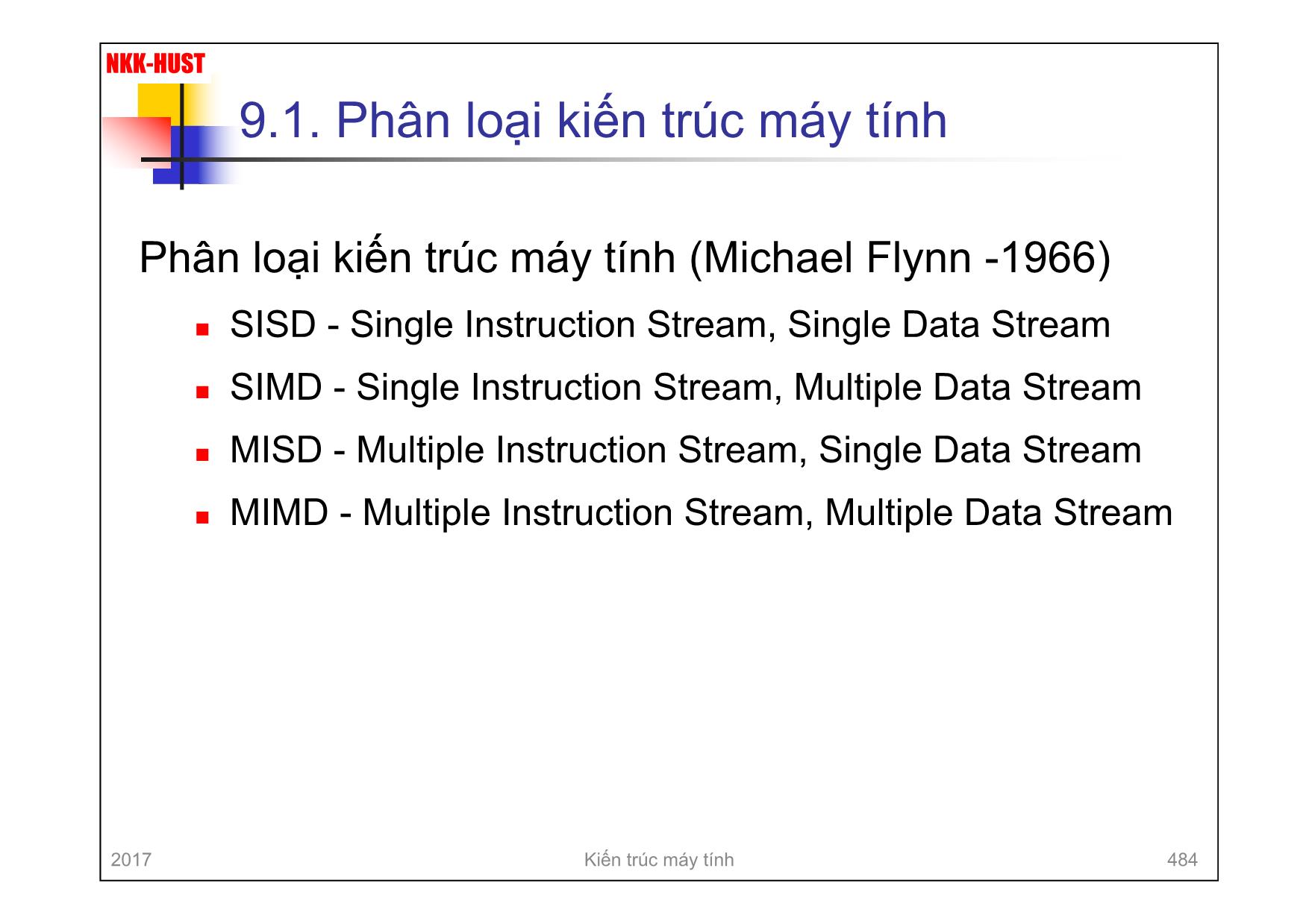
Phân loại kiến trúc máy tính (Michael Flynn -1966)
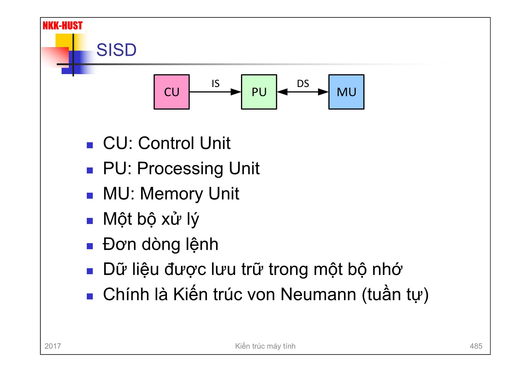
n SISD - Single Instruction Stream, Single Data Stream
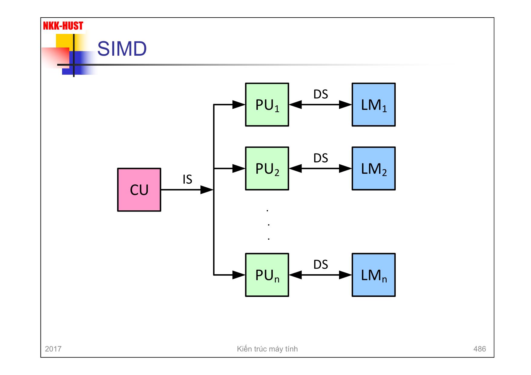
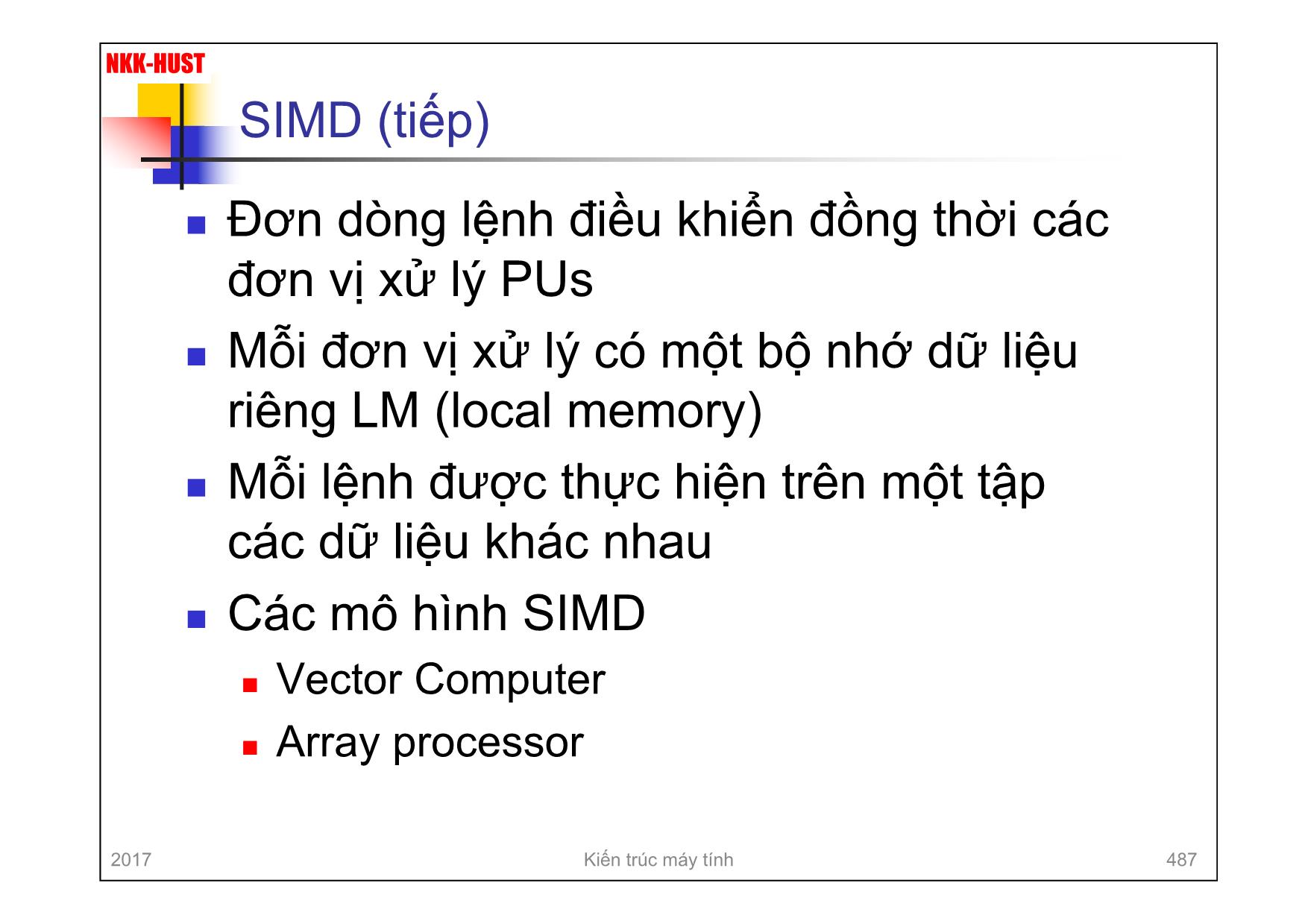
n SIMD - Single Instruction Stream, Multiple Data Stream
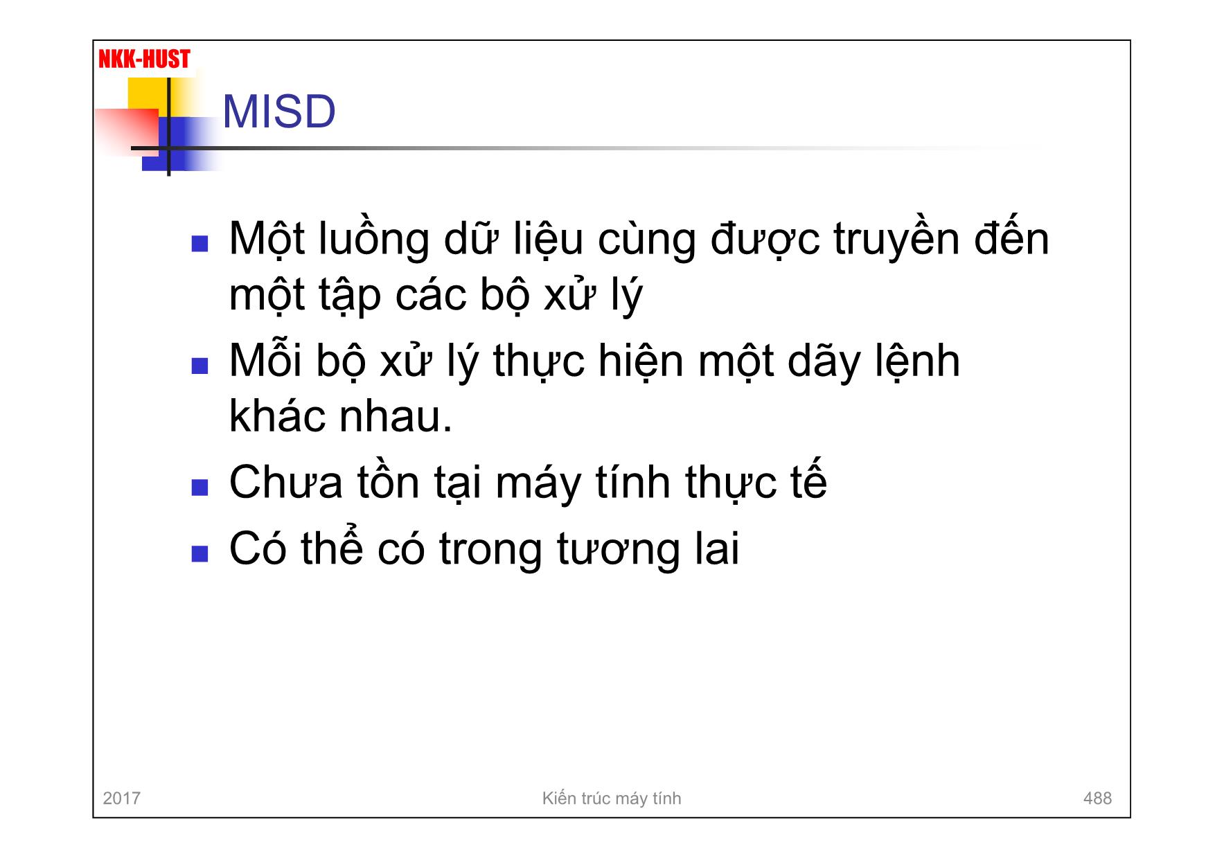
n MISD - Multiple Instruction Stream, Single Data Stream
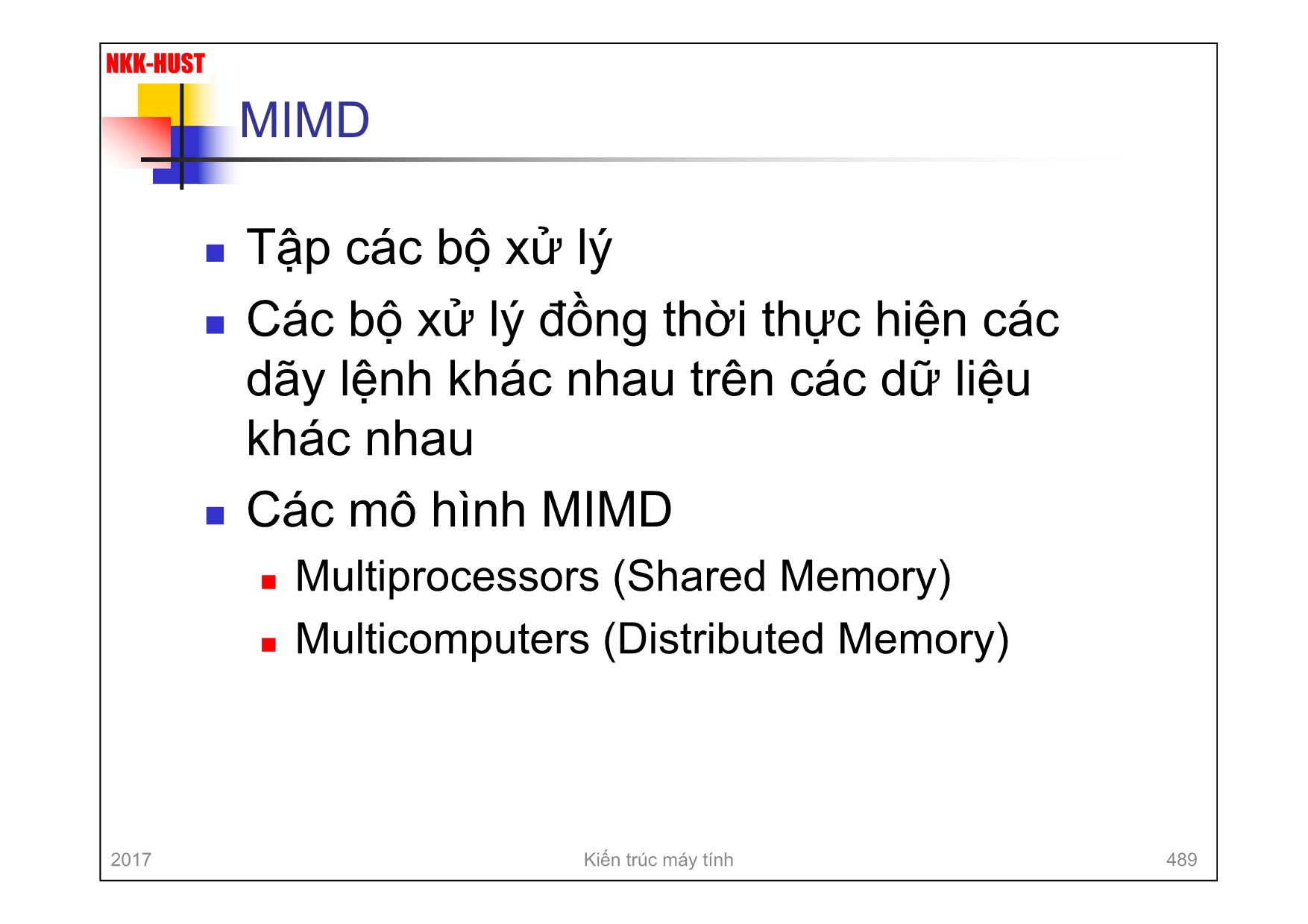
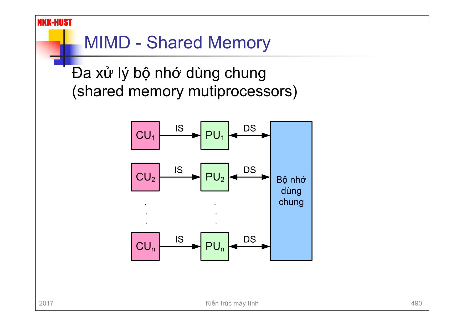
n MIMD - Multiple Instruction Stream, Multiple Data Stream

Trang 1

Trang 2

Trang 3
Trang 4
Trang 5
Trang 6
Trang 7
Trang 8
Trang 9
Trang 10
Tải về để xem bản đầy đủ
Bạn đang xem 10 trang mẫu của tài liệu "Bài giảng Kiến trúc máy tính - Chương 9: Các kiến trúc song song - Nguyễn Kim Khánh", để tải tài liệu gốc về máy hãy click vào nút Download ở trên
Tóm tắt nội dung tài liệu: Bài giảng Kiến trúc máy tính - Chương 9: Các kiến trúc song song - Nguyễn Kim Khánh

ors
digital sensors for high-accuracy die temperature measurements. Each core can
be defined as an independent thermal zone. The maximum temperature for each
Thermal control Thermal control
APIC APIC
32
-k
B
L1
 C
ac
he
s
32
-k
B
L1
 C
ac
he
s
Ex
ec
ut
io
n
re
so
u
rc
es
Ex
ec
ut
io
n
re
so
u
rc
es
A
rc
h.
 st
at
e
A
rc
h.
 st
at
e
Power management logic
2 MB L2 shared cache
Bus interface
Front-side bus
Figure 18.9 Intel Core Duo Block Diagram
2017 Kiến trúc máy tính 499
NKK-HUST
Intel Core i7-990X
678 CHAPTER 18 / MULTICORE COMPUTERS
The general structure of the Intel Core i7-990X is shown in Figure 18.10. Each
core has its own dedicated L2 cache and the four cores share a 12-MB L3 cache.
One mechanism Intel uses to make its caches more effective is prefetching, in which
the hardware examines memory access patterns and attempts to fill the caches spec-
ulatively with data that’s likely to be requested soon. It is interesting to compare the
performance of this three-level on chip cache organization with a comparable two-
level organization from Intel. Table 18.1 shows the cache access latency, in terms of
clock cycles for two Intel multicore systems running at the same clock frequency.
The Core 2 Quad has a shared L2 cache, similar to the Core Duo. The Core i7
improves on L2 cache performance with the use of the dedicated L2 caches, and
provides a relatively high-speed access to the L3 cache.
The Core i7-990X chip supports two forms of external communications to
other chips. The DDR3 memory controller brings the memory controller for the
DDR main memory2 onto the chip. The interface supports three channels that
are 8 bytes wide for a total bus width of 192 bits, for an aggregate data rate of
up to 32 GB/s. With the memory controller on the chip, the Front Side Bus is
eliminated.
Core 0
32 kB
L1-I
32 kB
L1-D
32 kB
L1-I
32 kB
L1-D
32 kB
L1-I
32 kB
L1-D
32 kB
L1-I
32 kB
L1-D
32 kB
L1-I
32 kB
L1-D
32 kB
L1-I
32 kB
L1-D
256 kB
L2 Cache
Core 1
256 kB
L2 Cache
Core 2
256 kB
L2 Cache
Core 3
256 kB
L2 Cache
Core 4
256 kB
L2 Cache
Core 5
256 kB
L2 Cache
12 MB
L3 Cache
DDR3 Memory
Controllers
QuickPath
Interconnect
3 ! 8B @ 1.33 GT/s 4 ! 20B @ 6.4 GT/s
Figure 18.10 Intel Core i7-990X Block Diagram
Table 18.1 Cache Latency (in clock cycles)
CPU Clock Frequency L1 Cache L2 Cache L3 Cache
Core 2 Quad 2.66 GHz 3 cycles 15 cycles —
Core i7 2.66 GHz 4 cycles 11 cycles 39 cycles
2The DDR synchronous RAM memory is discussed in Chapter 5.
2017 Kiến trúc máy tính 500
NKK-HUST
9.3. Đa xử lý bộ nhớ phân tán
n Máy tính qui mô lớn (Warehouse Scale Computers
or Massively Parallel Processors – MPP)
n Máy tính cụm (clusters)
SEC. 8.4 MESSAGE-PASSING MULTICOMPUTERS 617
As a consequence of these and other factors, there is a great deal of interest in
building and using parallel computers in which each CPU has its own private mem-
ory, not directly accessible to any other CPU. These are the multicomputers. Pro-
grams on multicomputer CPUs interact using primitives like send and receive to
explicitly pass messages because they cannot get at each other’s memory with
LOAD and STORE instructions. This difference completely changes the pro-
gramming model.
Each node in a multicomputer consists of one or a few CPUs, some RAM
(conceivably shared among the CPUs at that node only), a disk and/or other I/O de-
vices, and a communication processor. The communication processors are con-
nected by a high-speed interconnection network of the types we discussed in Sec.
8.3.3. Many different topologies, switching schemes, and routing algorithms are
used. What all multicomputers have in common is that when an application pro-
gram executes the send primitive, the communication processor is notified and
transmits a block of user data to the destination machine (possibly after first asking
for and getting permission). A generic multicomputer is shown in Fig. 8-36.
CPU Memory Node
Communication
processor
Local interconnect
Disk
and
I/O
Local interconnect
Disk
and
I/O
High-performance interconnection network
Figure 8-36. A generic multicomputer.
8.4.1 Interconnection Networks
In Fig. 8-36 we see that multicomputers are held together by interconnection
networks. Now it is time to look more closely at these interconnection networks.
Interestingly enough, multiprocessors and multicomputers are surprisingly similar
in this respect because multiprocessors often have multiple memory modules that
must also be interconnected with one another and with the CPUs. Thus the mater-
ial in this section frequently applies to both kinds of systems.
The fundamental reason why multiprocessor and multicomputer intercon-
nection networks are similar is that at the very bottom both of them use message
2017 Kiến trúc máy tính 501
NKK-HUST
Mạng liên kếtSEC. 8.4 MESSAGE-PASSING MULTICOMPUTERS 619
(a)
(c)
(e)
(g)
(b)
(d)
(f)
(h)
Figure 8-37. Various topologies. The heavy dots represent switches. The CPUs
and memories are not shown. (a) A star. (b) A complete interconnect. (c) A tree.
(d) A ring. (e) A grid. (f) A double torus. (g) A cube. (h) A 4D hypercube.
Interconnection networks can be characterized by their dimensionality . For
our purposes, the dimensionality is determined by the number of choices there are
to get from the source to the destination. If there is never any choice (i.e., there is
only one path from each source to each destination), the network is zero dimen-
sional. If there is one dimension in which a choice can be made, for example, go
2017 Kiến trúc máy tính 502
NKK-HUST
Massively Parallel Processors
n Hệ thống qui mô lớn
n Đắt tiền: nhiều triệu USD
n Dùng cho tính toán khoa học và các bài
toán có số phép toán và dữ liệu rất lớn
n Siêu máy tính
2017 Kiến trúc máy tính 503
NKK-HUST
IBM Blue Gene/P
624 PARALLEL COMPUTER ARCHITECTURES CHAP. 8
coherency between the L1 caches on the four CPUs. Thus when a shared piece of
memory resides in more than one cache, accesses to that storage by one processor
will be immediately visible to the other three processors. A memory reference that
misses on the L1 cache but hits on the L2 cache takes about 11 clock cycles. A
miss on L2 that hits on L3 takes about 28 cycles. Finally, a miss on L3 that has to
go to the main DRAM takes about 75 cycles.
The four CPUs are connected via a high-bandwidth bus to a 3D torus network,
which requires six connections: up, down, north, south, east, and west. In addition,
each processor has a port to the collective network, used for broadcasting data to
all processors. The barrier port is used to speed up synchronization operations, giv-
ing each processor fast access to a specialized synchronization network.
At the next level up, IBM designed a custom card that holds one of the chips
shown in Fig. 8-38 along with 2 GB of DDR2 DRAM. The chip and the card are
shown in Fig. 8-39(a)–(b) respectively.
1 Chip
4 CPUs
2 GB
4 processors
8-MB L3 cache
2-GB
DDR2
DRAM
32 Cards
32 Chips
128 CPUs
64 GB
32 Boards
1024 Cards
1024 Chips
4096 CPUs
2 TB
72 Cabinets
73728 Cards
73728 Chips
294912 CPUs
144 TB
SystemCabinetBoardCardChip:
(b) (c) (d) (e)(a)
Figure 8-39. The BlueGene/P: (a) chip. (b) card. (c) board. (d) cabinet.
(e) system.
The cards are mounted on plug-in boards, with 32 cards per board for a total of
32 chips (and thus 128 CPUs) per board. Since each card contains 2 GB of
DRAM, the boards contain 64 GB apiece. One board is illustrated in Fig. 8-39(c).
At the next level, 32 of these boards are plugged into a cabinet, packing 4096
CPUs into a single cabinet. A cabinet is illustrated in Fig. 8-39(d).
Finally, a full system, consisting of up to 72 cabinets with 294,912 CPUs, is
depicted in Fig. 8-39(e). A PowerPC 450 can issue up to 6 instructions/cycle, thus
2017 Kiến trúc máy tính 504
NKK-HUST
Cluster
n Nhiều máy tính được kết nối với nhau bằng
mạng liên kết tốc độ cao (~ Gbps)
n Mỗi máy tính có thể làm việc độc lập (PC
hoặc SMP)
n Mỗi máy tính được gọi là một node
n Các máy tính có thể được quản lý làm việc
song song theo nhóm (cluster)
n Toàn bộ hệ thống có thể coi như là một máy
tính song song
n Tính sẵn sàng cao
n Khả năng chịu lỗi lớn
2017 Kiến trúc máy tính 505
NKK-HUST
PC Cluster của Google SEC. 8.4 MESSAGE-PASSING MULTICOMPUTERS 635
hold exactly 80 PCs and switches can be larger or smaller than 128 ports; these are
just typical values for a Google cluster.
128-port Gigabit
Ethernet switch
128-port Gigabit
Ethernet switch
Two gigabit
Ethernet links
80-PC rack
OC-48 FiberOC-12 Fiber
Figure 8-44. A typical Google cluster.
Power density is also a key issue. A typical PC burns about 120 watts or about
10 kW per rack. A rack needs about 3 m2 so that maintenance personnel can in-
stall and remove PCs and for the air conditioning to function. These parameters
give a power density of over 3000 watts/m2. Most data centers are designed for
600–1200 watts/m2, so special measures are required to cool the racks.
Google has learned three key things about running massive Web servers that
bear repeating.
1. Components will fail so plan for it.
2. Replicate everything for throughput and availability.
3. Optimize price/performance.
2017 Kiến trúc máy tính 506
NKK-HUST
9.4. Bộ xử lý đồ họa đa dụng
n Kiến trúc SIMD
n Xuất phát từ bộ xử lý đồ họa GPU (Graphic
Processing Unit) hỗ trợ xử lý đồ họa 2D và
3D: xử lý dữ liệu song song
n GPGPU – General purpose Graphic
Processing Unit
n Hệ thống lai CPU/GPGPU
n CPU là host: thực hiện theo tuần tự
n GPGPU: tính toán song song
2017 Kiến trúc máy tính 507
NKK-HUST
Bộ xử lý đồ họa trong máy tính
2017 Kiến trúc máy tính 508
NKK-HUST
GPGPU: NVIDIA Tesla
nStreaming
multiprocessor
n8 × Streaming
processors
2017 Kiến trúc máy tính 509
NKK-HUST
GPGPU: NVIDIA Fermi
7
Hardware Execution
CUDA’s hierarchy of threads maps to a hierarchy of processors on the GPU; a GPU executes
one or more kernel grids; a streaming multiprocessor (SM) executes one or more thread blocks;
and CUDA cores and other execution units in the SM execute threads. The SM executes
threads in groups of 32 threads called a warp. While programmers can generally ignore warp
execution for functional correctness and think of programming one thread, they can greatly
improve performance by having threads in a warp execute the same code path and access
memory in nearby addresses.
An Overview of the Fermi Architecture
The first Fermi based GPU, implemented with 3.0 billion transistors, features up to 512 CUDA
cores. A CUDA core executes a floating point or integer instruction per clock for a thread. The
512 CUDA cores are organized in 16 SMs of 32 cores each. The GPU has six 64-bit memory
partitions, for a 384-bit memory interface, supporting up to a total of 6 GB of GDDR5 DRAM
memory. A host interface connects the GPU to the CPU via PCI-Express. The GigaThread
global scheduler distributes thread blocks to SM thread schedulers.
Fermi’s 16 SM are positioned around a common L2 cache. Each SM is a vertical
rectangular strip that contain an orange portion (scheduler and dispatch), a green portion
(execution units), and light blue portions (register file and L1 cache). 2017 Kiến trúc máy tính 510
NKK-HUST
NVIDIA Fermi
8
Third Generation Streaming
Multiprocessor
The third generation SM introduces several
architectural innovations that make it not only the
most powerful SM yet built, but also the most
programmable and efficient.
512 High Performance CUDA cores
Each SM features 32 CUDA
processors—a fourfold
increase over prior SM
designs. Each CUDA
processor has a fully
pipelined integer arithmetic
logic unit (ALU) and floating
point unit (FPU). Prior GPUs used IEEE 754-1985
floating point arithmetic. The Fermi architecture
implements the new IEEE 754-2008 floating-point
standard, providing the fused multiply-add (FMA)
instruction for both single and double precision
arithmetic. FMA improves over a multiply-add
(MAD) instruction by doing the multiplication and
addition with a single final rounding step, with no
loss of precision in the addition. FMA is more
accurate than performing the operations
separately. GT200 implemented double precision FMA.
In GT200, the integer ALU was limited to 24-bit precision for multiply operations; as a result,
multi-instruction emulation sequences were required for integer arithmetic. In Fermi, the newly
designed integer ALU supports full 32-bit precision for all instructions, consistent with standard
programming language requirements. The integer ALU is also optimized to efficiently support
64-bit and extended precision operations. Various instructions are supported, including
Boolean, shift, move, compare, convert, bit-field extract, bit-reverse insert, and population
count.
16 Load/Store Units
Each SM has 16 load/store units, allowing source and destination addresses to be calculated
for sixteen threads per clock. Supporting units load and store the data at each address to
cache or DRAM.
Dispatch Unit
Warp Scheduler
Instruction Cache
Dispatch Unit
Warp Scheduler
Core
Core Core
Core Core
Core Core
Core Core
Core Core
Core Core
Core Core
Core Core
Core Core
Core Core
Core Core
Core Core
Core Core
Core Core
Core Core
SFU
SFU
SFU
SFU
LD/ST
LD/ST
LD/ST
LD/ST
LD/ST
LD/ST
LD/ST
LD/ST
LD/ST
LD/ST
LD/ST
LD/ST
LD/ST
LD/ST
LD/ST
LD/ST
Interconnect Network
64 KB Shared Memory / L1 Cache
Uniform Cache
Core
Register File (32,768 x 32-bit)
CUDA Core
Operand Collector
Dispatch Port
Result Queue
FP Unit INT Unit
Fermi Streaming Multiprocessor (SM)
8
l i i i i i i
i l l i i
i i l i l ( )
i i i l l i i
i i . i l i l
( ) i i i l i li i
iti it i l fi l i t , it
l f r i i i t iti . i r
r t t rf r i t r ti
r t l . i l t l r i i .
I , t i t r li it t - it r i i f r lti l r ti ; r lt,
lti-i tr ti l ti r r ir f r i t r rit ti . I r i, t l
designed integer ALU supports full 32-bit precision fo r ll i tr ti , i t t it t r
r r i l r ir t . i t r i l ti i t ffi i tl rt
- it t r i i r ti . ri i tr ti r rt , i l i
l , ift, , r , rt, it-fi l tr t, it-r r i rt, l ti
t.
 / t r it
ach has 16 l a /st re units, all in s urce an estinati n a resses t e calculate
for sixteen threa s er clock. u orting units loa an store the ata at each a ress to
cache or .
r r r r
/
/
/
/
/
/
/
/
/
I t r t t r
64 are e ry / 1 ac e
if r ac e
lt
 i I i
r i tr i lti r r ( )
n Có 16 Streaming
Multiprocessors (SM)
n Mỗi SM có 32 CUDA
cores.
n Mỗi CUDA core
(Cumpute Unified
Device Architecture) có
01 FPU và 01 IU
2017 Kiến trúc máy tính 511
NKK-HUST
Hết
2017 Kiến trúc máy tính 512
File đính kèm:
 bai_giang_kien_truc_may_tinh_chuong_9_cac_kien_truc_song_son.pdf

