Bài giảng Kiến trúc máy tính - Chương 2: Cơ bản về logic số - Nguyễn Kim Khánh
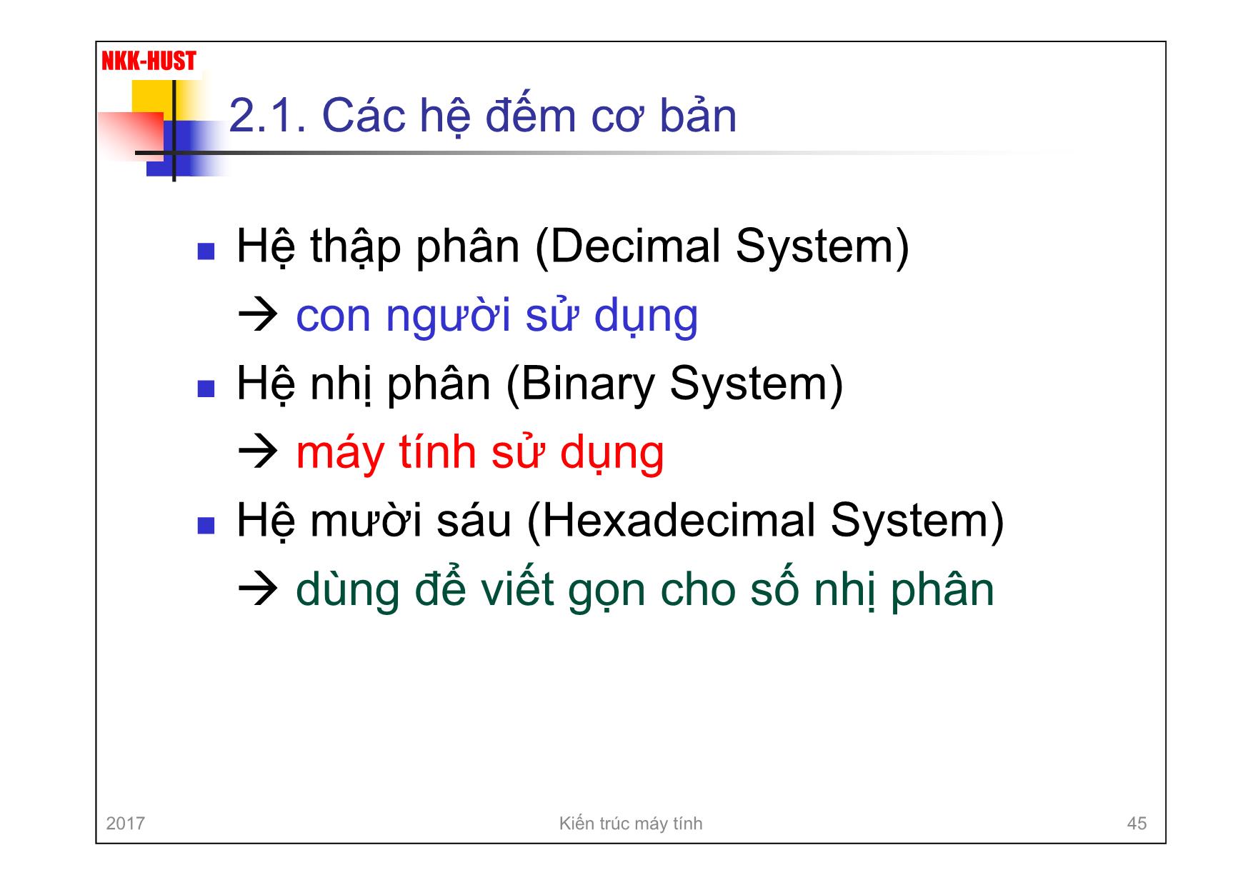
2.1. Các hệ đếm cơ bản
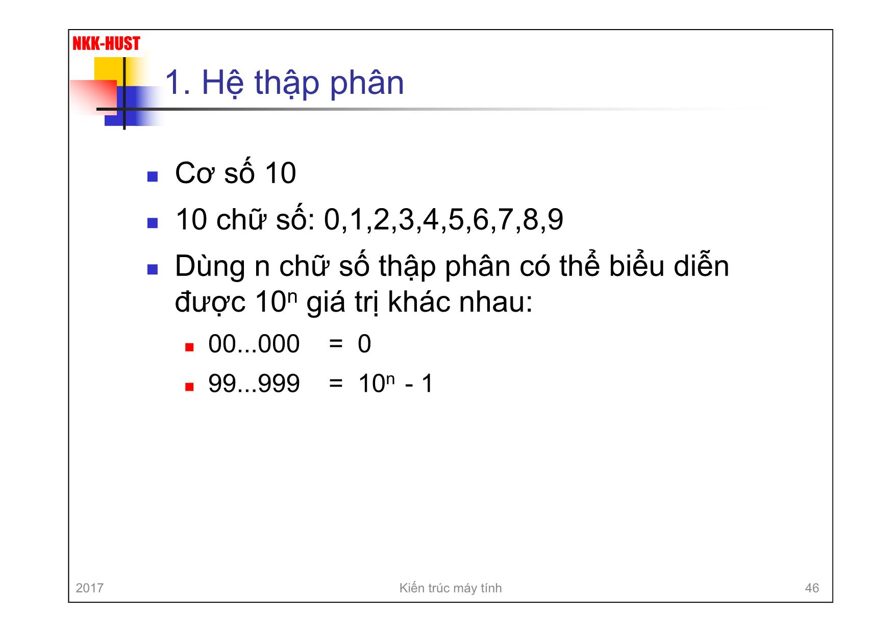
n Hệ thập phân (Decimal System)
à con người sử dụng
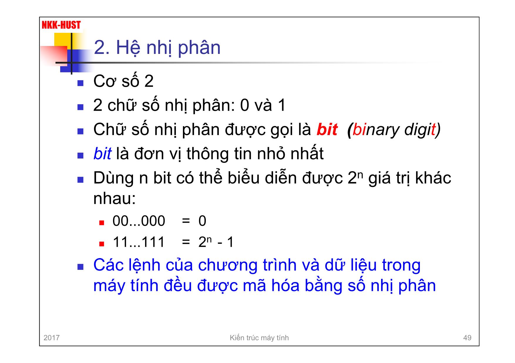
n Hệ nhị phân (Binary System)
à máy tính sử dụng
n Hệ mười sáu (Hexadecimal System)
à dùng để viết gọn cho số nhị phân
Trang 1
Trang 2
Trang 3
Trang 4
Trang 5
Trang 6
Trang 7
Trang 8
Trang 9
Trang 10
Tải về để xem bản đầy đủ
Bạn đang xem 10 trang mẫu của tài liệu "Bài giảng Kiến trúc máy tính - Chương 2: Cơ bản về logic số - Nguyễn Kim Khánh", để tải tài liệu gốc về máy hãy click vào nút Download ở trên
Tóm tắt nội dung tài liệu: Bài giảng Kiến trúc máy tính - Chương 2: Cơ bản về logic số - Nguyễn Kim Khánh

B16
8-bit
adder
A15
C7
B15
S15 S8
A8 B8
8-bit
adder
A7
Cin
B7
S7 S0
A0 B0
8-bit
adder
Figure 11.21 Construction of a 32-Bit Adder Using 8-Bit Adders
386 CHAPTER 11 / DIGITAL LOGIC
0 0 1 1
+0 +1 +0 +1
0 1 1 10
However, addition can still be dealt with in Boolean terms. In Table 11.9a, we
show the logic for adding two input bits to produce a 1-bit sum and a carry bit.
This truth table could easily be implemented in digital logic. However, we are not
interested in performing addition on just a single pair of bits. Rather, we wish to
add two n-bit numbers. This can be done by putting together a set of adders so that
the carry from one adder is provided as input to the next. A 4-bit adder is depicted
in Figure 11.19.
For a multiple-bit adder to work, each of the single-bit adders must have three
inputs, including the carry from the next-lower-order adder. The revised truth table
appears in Table 11.9b. The two outputs can be expressed:
Sum = A BC + ABC + ABC + ABC
Carry = AB + AC + BC
Figure 11.20 is an implementation using AND, OR, and NOT gates.
A3
C3
S3
Cin
B3 A2
C2
S2
Cin
B2 A1
C1
S1
Cin
B1 A0
C0
S0
Cin 0
B0
Overflow
signal
Figure 11.19 4-Bit Adder
Table 11.9 Binary Addition Truth Tables
(a) Single-Bit Addition
A B Sum Carry
0 0 0 0
0 1 1 0
1 0 1 0
1 1 0 1
(b) Addition with Carry Input
Cin A B Sum Cout
0 0 0 0 0
0 0 1 1 0
0 1 0 1 0
0 1 1 0 1
1 0 0 1 0
1 0 1 0 1
1 1 0 0 1
1 1 1 1 1
2017 Kiến trúc máy tính 81
NKK-HUST
2.5. Mạch dãy
n Mạch dãy là mạch logic trong đó đầu ra phụ
thuộc giá trị đầu vào ở thời điểm hiện tại và
đầu vào ở thời điểm quá khứ
n Là mạch có nhớ, được thực hiện bằng phần
tử nhớ (Latch, Flip-Flop) và có thể kết hợp
với các cổng logic
2017 Kiến trúc máy tính 82
NKK-HUST
Các Flip-Flop cơ bản
392 CHAPTER 11 / DIGITAL LOGIC
Name Graphical Symbol Truth Table
S–R
S Q
R Q
S R
0 0
0
1
1
Qn
Qn!1
1
0
–
0
1
1
J–K
J Q
K Q
J K
0 0
0
1
1
Qn
Qn
Qn!1
1
00
1
1
D
D Q
Q
D
0 0
1
Qn!1
1
Ck
Ck
Ck
Figure 11.27 Basic Flip-Flops
causing the output to be 1; if only the K input is asserted, the result is a reset function,
causing the output to be 0. When both J and K are 1, the function performed is
referred to as the toggle function: the output is reversed. Thus, if Q is 1 and 1 is applied
to J and K, then Q becomes 0. The reader should verify that the implementation of
Figure 11.26 produces this characteristic function.
J
K
Q
Q
Clock
Figure 11.26 J–K Flip-Flop
2017 Kiến trúc máy tính 83
NKK-HUST
S-R Latch và các Flip-Flop
S-R Latch S-R Flip-Flop
J-K Flip-FlopD Flip Flop
2017 Kiến trúc máy tính 84
11.4 / SEQUENTIAL CIRCUITS 389
First, let us show that the circuit is bistable. Assume that both S and R are 0
and that Q is 0. The inputs to the lower NOR gate are Q = 0 and S = 0. Thus, the
output Q = 1 means that the inputs to the upper NOR gate are Q = 1 and R = 0,
which has the output Q = 0. Thus, the state of the circuit is internally consistent
and remains stable as long as S = R = 0. A similar line of reasoning shows that the
state Q = 1, Q = 0 is also stable for R = S = 0.
Thus, this circuit can function as a 1-bit memory. We can view the output Q as
the “value” of the bit. The inputs S and R serve to write the values 1 and 0, respec-
tively, into memory. To see this, consider the state Q = 0, Q = 1, S = 0, R = 0.
Suppose that S changes to the value 1. Now the inputs to the lower NOR gate are
S = 1, Q = 0. After some time delay ^t, the output of the lower NOR gate will be
Q = 0 (see Figure 11.23). So, at this point in time, the inputs to the upper NOR gate
become R = 0, Q = 0. After another gate delay of ^t the output Q becomes 1. This
is again a stable state. The inputs to the lower gate are now S = 1, Q = 1, which
maintain the output Q = 0. As long as S = 1 and R = 0, the outputs will remain
Q = 1, Q = 0. Furthermore, if S returns to 0, the outputs will remain unchanged.
The R output performs the opposite function. When R goes to 1, it forces
Q = 0, Q = 1 regardless of the previous state of Q and Q. Again, a time delay of
2^t occurs before the final state is established (Figure 11.23).
The S–R latch can be defined with a table similar to a truth table, called a
characteristic table, which shows the next state or states of a sequential circuit as
a function of current states and inputs. In the case of the S–R latch, the state can
be defined by the value of Q. Table 11.10a shows the resulting characteristic table.
Observe that the inputs S = 1, R = 1 are not allowed, because these would pro-
duce an inconsistent output (both Q and Q equal 0). The table can be expressed
more compactly, as in Table 11.10b. An illustration of the behavior of the S–R latch
is shown in Table 11.10c.
S
Q
Q
R
Figure 11.22 The S–R Latch Implemented
with NOR Gates
CLOCKED S–R FLIP-FLOP The output of the S–R latch changes, after a brief
time delay, in response to a change in the input. This is referred to as asynchronous
operation. More typically, events in the digital computer are synchronized to a clock
pulse, so that changes occur only when a clock pulse occurs. Figure 11.24 shows this
11.4 / SEQUENTIAL CIRCUITS 391
arrangement. This device is referred to as a clocked S–R flip-flop. Note that the
R and S inputs are passed to the NOR gates only during the clock pulse.
D FLIP-FLOP One problem with S–R flip-flop is that the condition R = 1, S = 1
must be avoided. One way to do this is to allow just a single input. The D flip-flop
accomplishes this. Figure 11.25 shows a gate implementation of the D flip-flop. By
using an inverter, the nonclock inputs to the two AND gates are guaranteed to be
the opposite of each other.
The D flip-flop is sometimes referred to as the data flip-flop because it is, in
effect, storage for one bit of data. The output of the D flip-flop is always equal to the
most recent value applied to the input. Hence, it remembers and produces the last
input. It is also referred to as the delay flip-flop, because it delays a 0 or 1 applied to
its input for a single clock pulse. We can capture the logic of the D flip-flop in the
following truth table:
D Qn!1
0 0
1 1
J–K FLIP-FLOP Another useful flip-flop is the J–K flip-flop. Like the S–R flip-flop,
it has two inputs. However, in this case all possible combinations of input values are
valid. Figure 11.26 shows a gate implementation of the J–K flip-flop, and Figure 11.27
shows its characteristic table (along with those for the S–R and D flip-flops). Note
that the first three combinations are the same as for the S–R flip-flop. With no input
asserted, the output is stable. If only the J input is asserted, the result is a set function,
S
R
Q
Q
Clock
Figure 11.24 Clocked S–R Flip-Flop
D
Q
Q
Clock
Figure 11.25 D Flip-Flop
11.4 / SEQUENTIAL CIRCUITS 391
arr ngement. This device is referred to as a clocked S–R flip-flop. Note th t the
R and S inputs are passed to the NOR gates only during the clock p lse.
D FLIP-FLOP One problem with S–R flip-flop is that the condition R = 1, S = 1
must be avoided. One way to do this is to allow just a single input. The D flip-flop
accomplishes this. Figure 11.25 shows a gate implementation of the D flip-flop. By
using an inverter, the nonclock inputs to the two AND gates are guaranteed to be
the opposite of each other.
The D flip-flop is sometimes referred to as the data flip-flop because it is, in
effect, storage for one bit of data. The output of the D flip-flop is always equal to the
most recent value applied to the input. Hence, it remembers and produces the last
input. It is also referred to as the delay flip-flop, because it delays a 0 or 1 applied to
its input for a single clock pulse. We can capture the logic of the D flip-flop in the
following truth table:
D Qn!1
0 0
1 1
J–K FLIP-FLOP Another useful flip-flop is the J–K flip-flop. Like the S–R flip-flop,
it has two inputs. However, in this case all possible combinations of input values are
valid. Figure 11.26 shows a gate implementation of the J–K flip-flop, and Figure 11.27
shows its characteristic table (along with those for the S–R and D flip-flops). Note
that the first three combinations are the same as for the S–R flip-flop. With no input
asserted, the output is stable. If only the J input is asserted, the result is a set function,
S
R
Q
Q
Clock
Figure 11.24 Clocked S–R Flip-Flop
D
Q
Q
Clock
Figure 11.25 D Flip-Flop
392 CHAPTER 11 / DIGITAL LOGIC
Name Graphical Symbol Truth Table
S–R
S Q
R Q
S R
0 0
0
1
1
Qn
Qn!1
1
0
–
0
1
1
J–K
J Q
K Q
J K
0 0
0
1
1
Qn
Qn
Qn!1
1
00
1
1
D
D Q
Q
D
0 0
1
Qn!1
1
Ck
Ck
Ck
Figure 11.27 Basic Flip-Flops
causing the output to be 1; if only the K input is asserted, the result is a reset function,
causing the output to be 0. When both J and K are 1, the function performed is
referred to as the toggle function: the output is reversed. Thus, if Q is 1 and 1 is applied
to J and K, then Q becomes 0. The reader should verify that the implementation of
Figure 11.26 produces this characteristic function.
J
K
Q
Q
Clock
Figure 11.26 J–K Flip-Flop
NKK-HUST
Thanh ghi 8-bit song song
11.4 / SEQUENTIAL CIRCUITS 393
Registers
As an example of the use of flip-flops, let us first examine one of the essential ele-
ments of the CPU: the register. As we know, a register is a digital circuit used within
the CPU to store one or more bits of data. Two basic types of registers are com-
monly used: parallel registers and shift registers.
PARALLEL EGISTERS A parallel register consists of a set of 1-bit memories that
can be read or written simultaneously. It is used to store data. The registers that we
have discussed throughout this book are parallel registers.
The 8-bit register of Figure 11.28 illustrates the operation of a parallel register
using D flip-flops. A control signal, labeled load, controls writing into the register
from signal lines, D11 through D18. These lines might be the output of multiplexers,
so that data from a variety of sources can be loaded into the register.
SHIFT REGISTER A shift register accepts and/or transfers information serially.
Consider, for example, Figure 11.29, which shows a 5-bit shift register constructed
from clocked D flip-flops. Data are input only to the leftmost flip-flop. With each
clock pulse, data are shifted to the right one position, and the rightmost bit is
transferred out.
Shift registers can be used to interface to serial I/O devices. In addition, they
can be used within the ALU to perform logical shift and rotate functions. In this
D
D08
D18
Clk
Q D
Clk
Q D
Clk
Q D
Clk
Q D
Clk
Q D
Clk
Q D
Clk
Q D
Clk
Q
Clock
Load
D17 D16 D15 D14 D13 D12 D11
D07 D06 D05
Output lines
Data lines
D04 D03 D02 D01
Figure 11.28 8-Bit Parallel Register
D
Clk
Q D
Clk
Q D
Clk
Q D
Clk
Q D
Clk
Q
Clock
Serial in Serial out
Figure 11.29 5-Bit Shift Register
2017 Kiến trúc máy tính 85
NKK-HUST
Thanh ghi dịch 5-bit
11.4 / SEQUENTIAL CIRCUITS 393
Registers
As an example of the use of flip-flops, let us first examine one of the essential ele-
ments of the CPU: the register. As we know, a register is a digital circuit used within
the CPU to store one or more bits of data. Two basic types of registers are com-
monly used: parallel registers and shift registers.
PARALLEL REGISTERS A parallel register consists of a set of 1-bit memories that
can be read or written simultaneously. It is used to store data. The registers that we
have discussed throughout this book are parallel registers.
The 8-bit register of Figure 11.28 illustrates the operation of a parallel register
using D flip-flops. A control signal, labeled load, controls writing into the register
from signal lines, D11 through D18. These lines might be the output of multiplexers,
so that data from a variety of sources can be loaded into the register.
SHIFT REGISTER A shift register accepts and/or transfers information serially.
Consider, for example, Figure 11.29, which shows a 5-bit shift register constructed
from clocked D flip-flops. Data are input only to the leftmost flip-flop. With each
clock pulse, data are shifted to the right one position, and the rightmost bit is
transferred out.
Shift registers can be used to interface to serial I/O devices. In addition, they
can be used within the ALU to perform logical shift and rotate functions. In this
D
D08
D18
Clk
Q D
Clk
Q D
Clk
Q D
Clk
Q D
Clk
Q D
Clk
Q D
Clk
Q D
Clk
Q
Clock
Load
D17 D16 D15 D14 D13 D12 D11
D07 D06 D05
Output lines
Data lines
D04 D03 D02 D01
Figure 11.28 8-Bit Parallel Register
D
Clk
Q D
Clk
Q D
Clk
Q D
Clk
Q D
Clk
Q
Clock
Serial in Serial out
Figure 11.29 5-Bit Shift Register
2017 Kiến trúc máy tính 86
NKK-HUST
Bộ đếm 4-bit
394 CHAPTER 11 / DIGITAL LOGIC
latter capacity, they need to be equipped with parallel read/write circuitry as well
as serial.
Counters
Another useful category of sequential circuit is the counter. A counter is a register
whose value is easily incremented by 1 modulo the capacity of the register; that is,
after the maximum value is achieved the next increment sets the counter value to 0.
Thus, a register made up of n flip-flops can count up to 2n - 1. An example of a
counter in the CPU is the program counter.
Counters can be designated as asynchronous or synchronous, depending on
the way in which they operate. Asynchronous counters are relatively slow because
the output of one flip-flop triggers a change in the status of the next flip-flop. In a
synchronous counter, all of the flip-flops change state at the same time. Because the
latter type is much faster, it is the kind used in CPUs. However, it is useful to begin
the discussion with a description of an asynchronous counter.
RIPPLE COUNTER An asynchronous counter is also referred to as a ripple counter,
because the change that occurs to increment the counter starts at one end and
“ripples” through to the other end. Figure 11.30 shows an implementation of a
4-bit counter using J–K flip-flops, together with a timing diagram that illustrates its
behavior. The timing diagram is idealized in that it does not show the propagation
delay that occurs as the signals move down the series of flip-flops. The output of
the leftmost flip-flop (Q0) is the least significant bit. The design could clearly be
extended to an arbitrary number of bits by cascading more flip-flops.
J Q
Q0
Q0
Q1
Q2
Q3
K Q
Ck
J Q
Q1
K Q
Ck
J Q
Q2
K Q
Ck
J Q
Q3
K Q
CkClock
Clock
High
(a) Sequential circuit
(b) Timing diagram
Figure 11.30 Ripple Counter
2017 Kiến trúc máy tính 87
NKK-HUST
Hết chương 2
2017 Kiến trúc máy tính 88
File đính kèm:
 bai_giang_kien_truc_may_tinh_chuong_2_co_ban_ve_logic_so_ngu.pdf

