Combined power ratio calculation, hadamard transform and lms - Based calibration of channel mismatches in time - interleaved adcs
This paper presents a method for all-digital background calibration of multiple channel
mismatches including offset, gain and timing mismatches in time-interleaved analog-to-digital
converters (TIADCs). The average technique is used to remove offset mismatch at each channel.
The gain mismatch is calibrated by calculating the power ratio of the sub-ADC over the reference
ADC. The timing skew mismatch is calibrated by using Hadamard transform for error correction
and LMS for timing mismatch estimation. The performance improvement of TIADCs employing
these techniques is demonstrated through numerical simulations. Besides, achievement results on
the field-programmable gate array (FPGA) hardware have demonstrated the effectiveness of the
proposed techniques.

Trang 1
Trang 2
Trang 3
Trang 4
Trang 5
Trang 6
Trang 7
Trang 8
Trang 9
Trang 10
Tải về để xem bản đầy đủ
Tóm tắt nội dung tài liệu: Combined power ratio calculation, hadamard transform and lms - Based calibration of channel mismatches in time - interleaved adcs
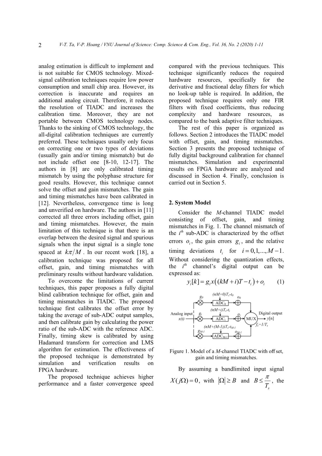
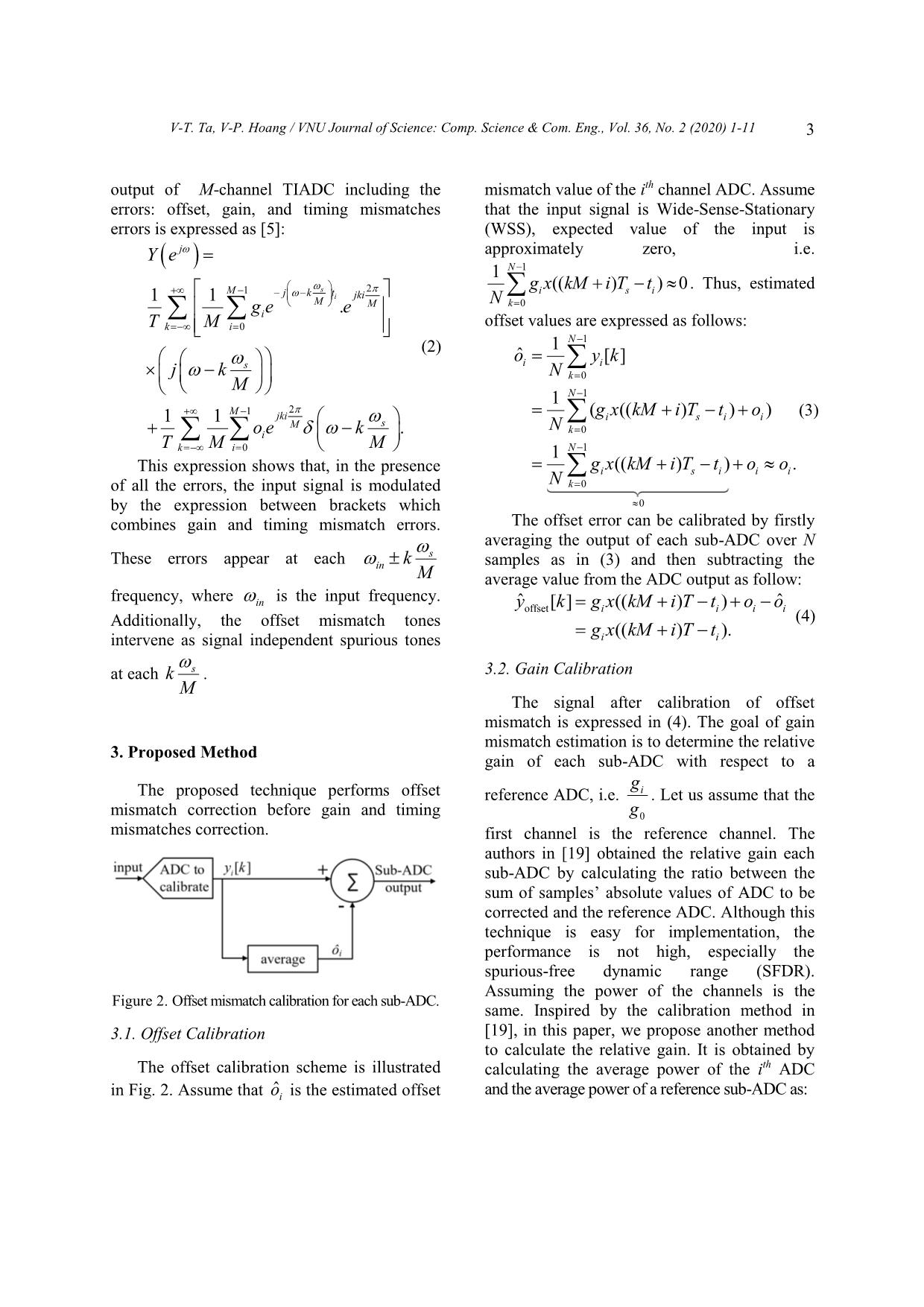
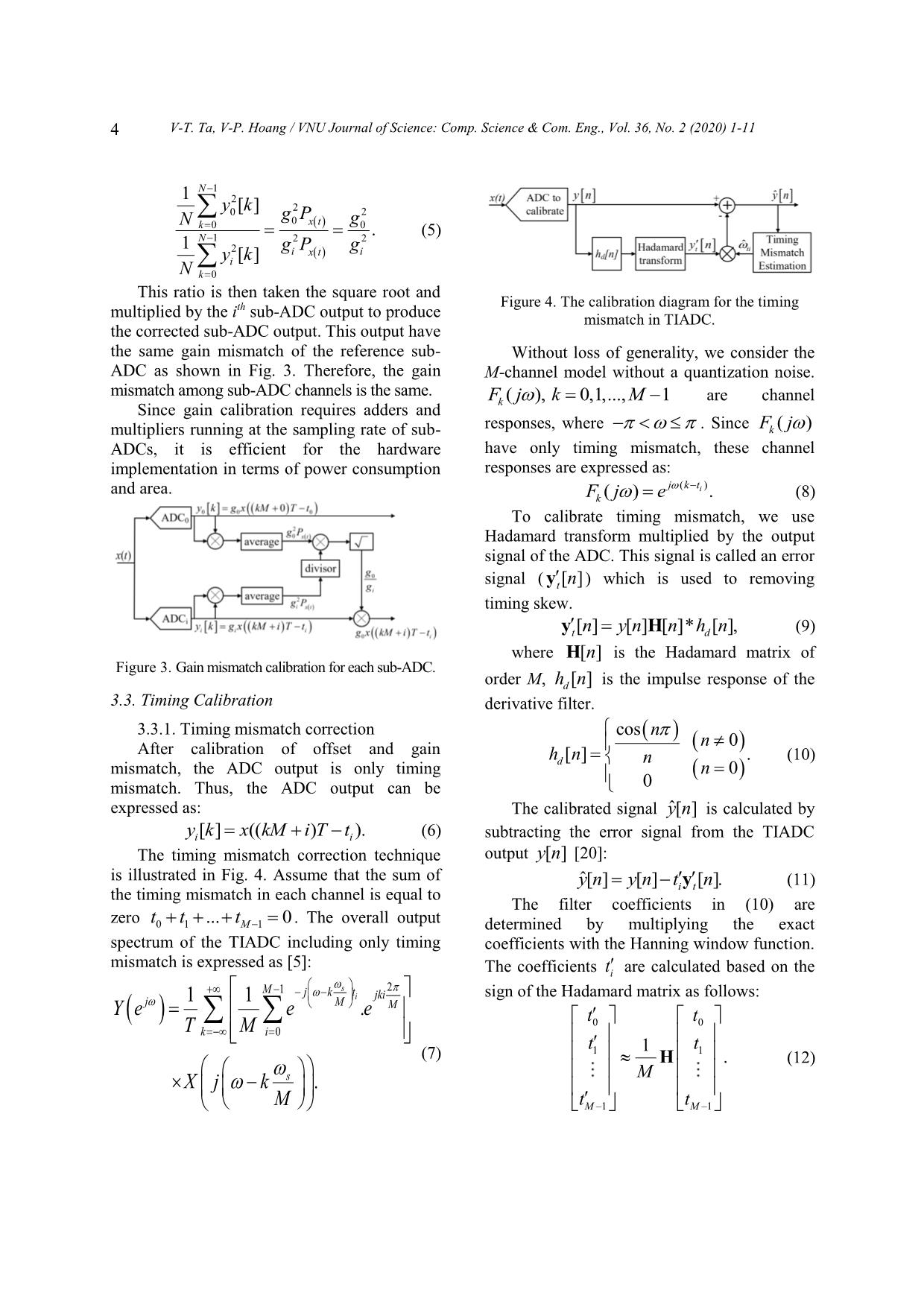
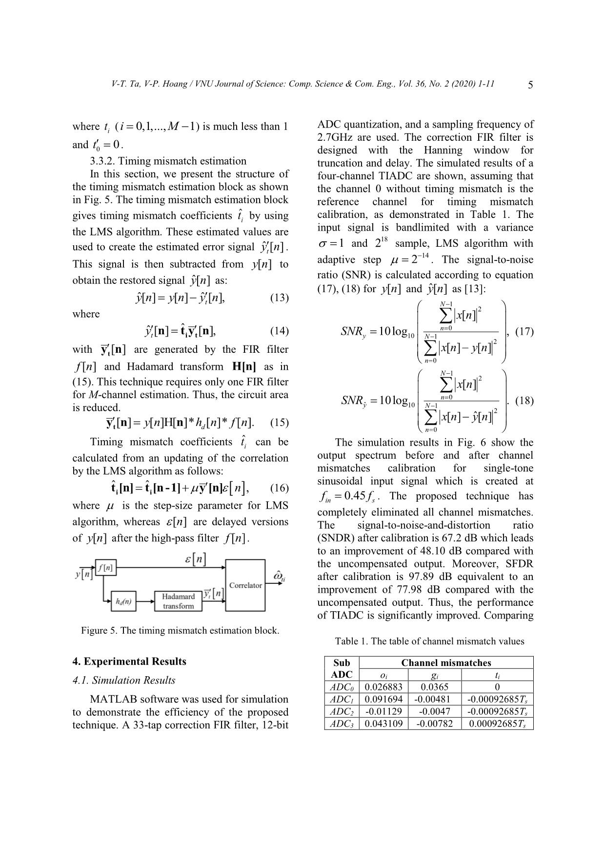
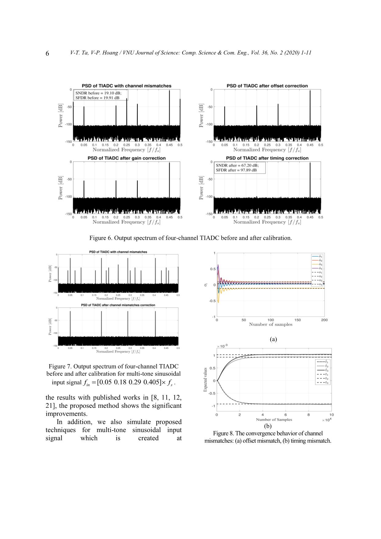
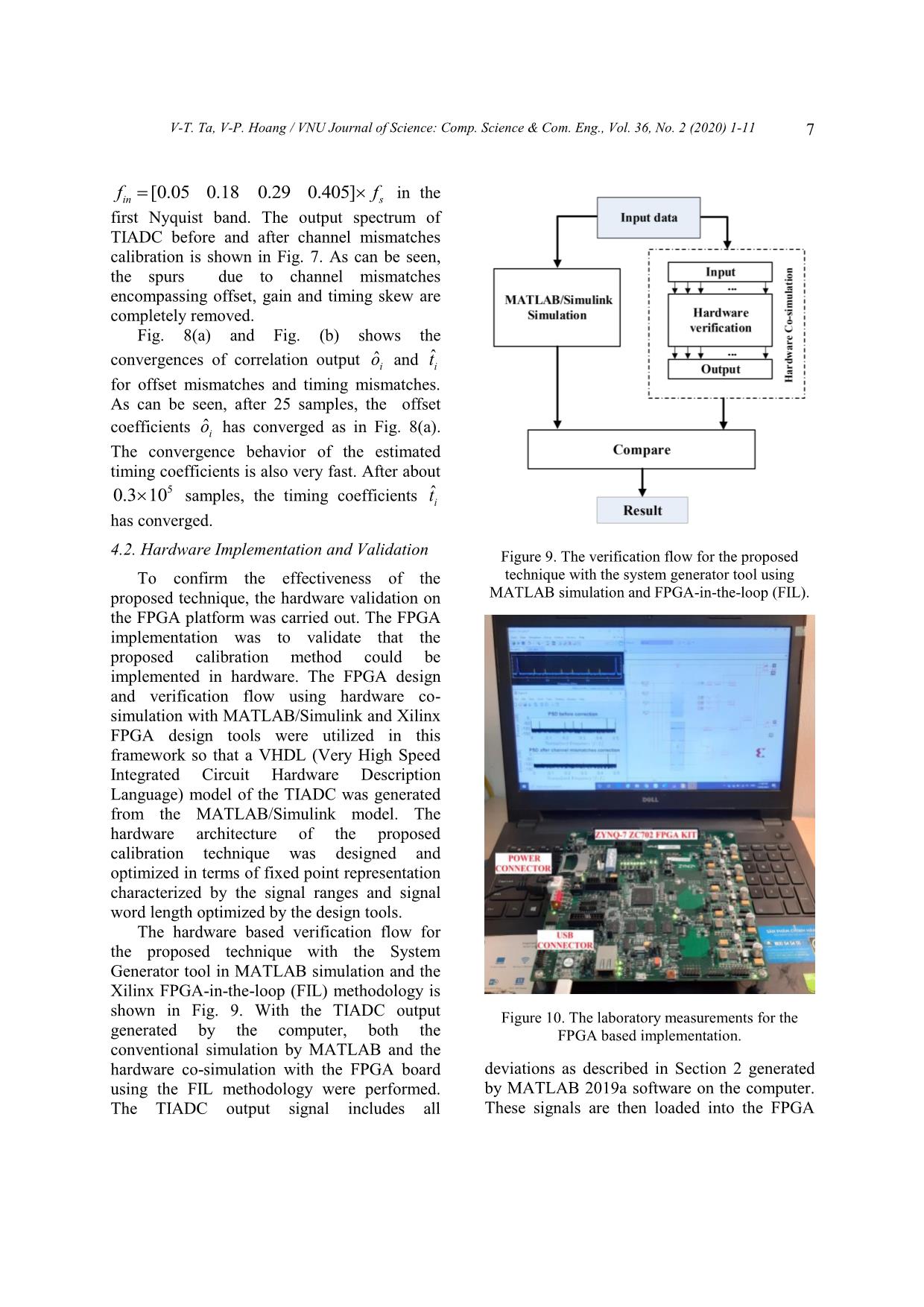
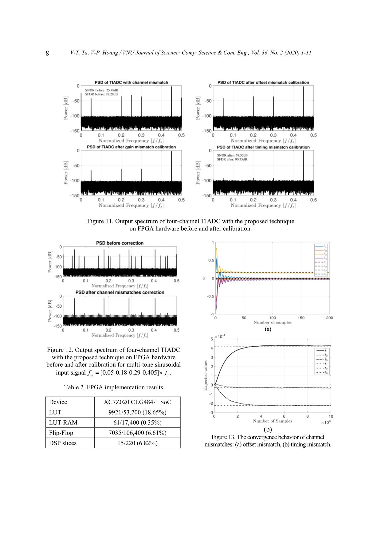
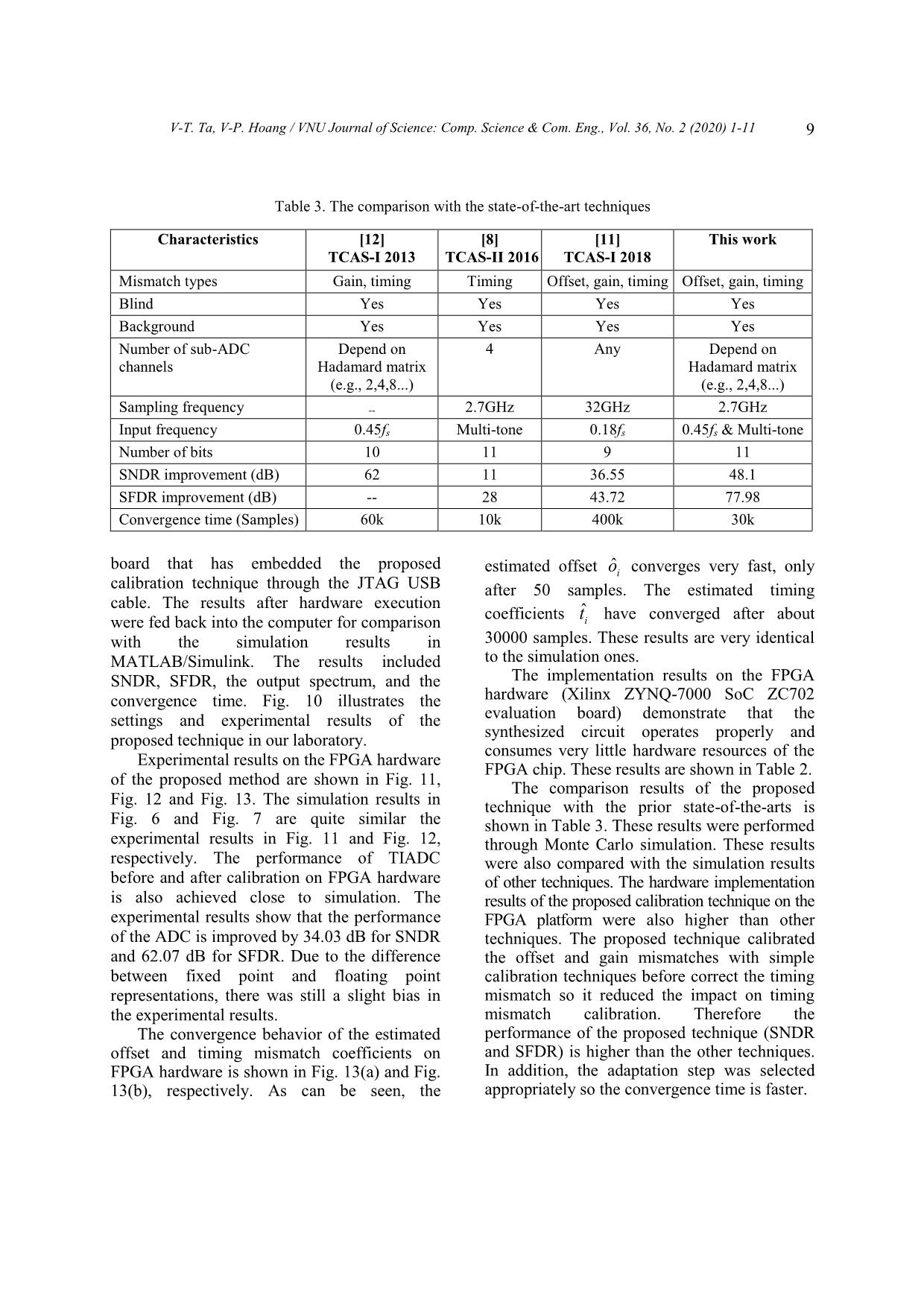
el estimation. Thus, the circuit area is reduced. [ ] [ ]H[ ]* [ ]* [ ].dy n h n f n ty n n (15) Timing mismatch coefficients iˆt can be calculated from an updating of the correlation by the LMS algorithm as follows: ˆ ˆ ,n i i[n] [n -1 y [n]t t ] (16) where is the step-size parameter for LMS algorithm, whereas [ ]n are delayed versions of [ ]y n after the high-pass filter [ ]f n . Figure 5. The timing mismatch estimation block. 4. Experimental Results 4.1. Simulation Results MATLAB software was used for simulation to demonstrate the efficiency of the proposed technique. A 33-tap correction FIR filter, 12-bit ADC quantization, and a sampling frequency of 2.7GHz are used. The correction FIR filter is designed with the Hanning window for truncation and delay. The simulated results of a four-channel TIADC are shown, assuming that the channel 0 without timing mismatch is the reference channel for timing mismatch calibration, as demonstrated in Table 1. The input signal is bandlimited with a variance 1 and 182 sample, LMS algorithm with adaptive step 142 . The signal-to-noise ratio (SNR) is calculated according to equation (17), (18) for [ ]y n and ˆ[ ]y n as [13]: 1 2 0 10 1 2 0 [ ] [ ] ,10lo [ ] g N n y N n x S n nx y n NR (17) 1 2 0 ˆ 10 1 2 0 [ ] [ ] .0 [ 1 og ] l ˆ N n y N n x n S nx y n NR (18) The simulation results in Fig. 6 show the output spectrum before and after channel mismatches calibration for single-tone sinusoidal input signal which is created at 0.45in sf f . The proposed technique has completely eliminated all channel mismatches. The signal-to-noise-and-distortion ratio (SNDR) after calibration is 67.2 dB which leads to an improvement of 48.10 dB compared with the uncompensated output. Moreover, SFDR after calibration is 97.89 dB equivalent to an improvement of 77.98 dB compared with the uncompensated output. Thus, the performance of TIADC is significantly improved. Comparing Table 1. The table of channel mismatch values Sub ADC Channel mismatches oi gi ti ADC0 0.026883 0.0365 0 ADC1 0.091694 -0.00481 -0.00092685Ts ADC2 -0.01129 -0.0047 -0.00092685Ts ADC3 0.043109 -0.00782 0.00092685Ts V-T. Ta, V-P. Hoang / VNU Journal of Science: Comp. Science & Com. Eng., Vol. 36, No. 2 (2020) 1-11 6 Figure 6. Output spectrum of four-channel TIADC before and after calibration. Figure 7. Output spectrum of four-channel TIADC before and after calibration for multi-tone sinusoidal input signal [0.05 0.18 0.29 0.405]in sf f . the results with published works in [8, 11, 12, 21], the proposed method shows the significant improvements. In addition, we also simulate proposed techniques for multi-tone sinusoidal input signal which is created at (a) (b) Figure 8. The convergence behavior of channel mismatches: (a) offset mismatch, (b) timing mismatch. V-T. Ta, V-P. Hoang / VNU Journal of Science: Comp. Science & Com. Eng., Vol. 36, No. 2 (2020) 1-11 7 [0.05 0.18 0.29 0.405]in sf f in the first Nyquist band. The output spectrum of TIADC before and after channel mismatches calibration is shown in Fig. 7. As can be seen, the spurs due to channel mismatches encompassing offset, gain and timing skew are completely removed. Fig. 8(a) and Fig. (b) shows the convergences of correlation output ˆio and iˆt for offset mismatches and timing mismatches. As can be seen, after 25 samples, the offset coefficients ˆio has converged as in Fig. 8(a). The convergence behavior of the estimated timing coefficients is also very fast. After about 50.3 10 samples, the timing coefficients iˆt has converged. 4.2. Hardware Implementation and Validation To confirm the effectiveness of the proposed technique, the hardware validation on the FPGA platform was carried out. The FPGA implementation was to validate that the proposed calibration method could be implemented in hardware. The FPGA design and verification flow using hardware co- simulation with MATLAB/Simulink and Xilinx FPGA design tools were utilized in this framework so that a VHDL (Very High Speed Integrated Circuit Hardware Description Language) model of the TIADC was generated from the MATLAB/Simulink model. The hardware architecture of the proposed calibration technique was designed and optimized in terms of fixed point representation characterized by the signal ranges and signal word length optimized by the design tools. The hardware based verification flow for the proposed technique with the System Generator tool in MATLAB simulation and the Xilinx FPGA-in-the-loop (FIL) methodology is shown in Fig. 9. With the TIADC output generated by the computer, both the conventional simulation by MATLAB and the hardware co-simulation with the FPGA board using the FIL methodology were performed. The TIADC output signal includes all Figure 9. The verification flow for the proposed technique with the system generator tool using MATLAB simulation and FPGA-in-the-loop (FIL). Figure 10. The laboratory measurements for the FPGA based implementation. deviations as described in Section 2 generated by MATLAB 2019a software on the computer. These signals are then loaded into the FPGA V-T. Ta, V-P. Hoang / VNU Journal of Science: Comp. Science & Com. Eng., Vol. 36, No. 2 (2020) 1-11 8 Figure 11. Output spectrum of four-channel TIADC with the proposed technique on FPGA hardware before and after calibration. Figure 12. Output spectrum of four-channel TIADC with the proposed technique on FPGA hardware before and after calibration for multi-tone sinusoidal input signal [0.05 0.18 0.29 0.405]in sf f . Table 2. FPGA implementation results Device XC7Z020 CLG484-1 SoC LUT 9921/53,200 (18.65%) LUT RAM 61/17,400 (0.35%) Flip-Flop 7035/106,400 (6.61%) DSP slices 15/220 (6.82%) (a) (b) Figure 13. The convergence behavior of channel mismatches: (a) offset mismatch, (b) timing mismatch. V-T. Ta, V-P. Hoang / VNU Journal of Science: Comp. Science & Com. Eng., Vol. 36, No. 2 (2020) 1-11 9 Table 3. The comparison with the state-of-the-art techniques Characteristics [12] TCAS-I 2013 [8] TCAS-II 2016 [11] TCAS-I 2018 This work Mismatch types Gain, timing Timing Offset, gain, timing Offset, gain, timing Blind Yes Yes Yes Yes Background Yes Yes Yes Yes Number of sub-ADC channels Depend on Hadamard matrix (e.g., 2,4,8...) 4 Any Depend on Hadamard matrix (e.g., 2,4,8...) Sampling frequency -- 2.7GHz 32GHz 2.7GHz Input frequency 0.45fs Multi-tone 0.18fs 0.45fs & Multi-tone Number of bits 10 11 9 11 SNDR improvement (dB) 62 11 36.55 48.1 SFDR improvement (dB) -- 28 43.72 77.98 Convergence time (Samples) 60k 10k 400k 30k board that has embedded the proposed calibration technique through the JTAG USB cable. The results after hardware execution were fed back into the computer for comparison with the simulation results in MATLAB/Simulink. The results included SNDR, SFDR, the output spectrum, and the convergence time. Fig. 10 illustrates the settings and experimental results of the proposed technique in our laboratory. Experimental results on the FPGA hardware of the proposed method are shown in Fig. 11, Fig. 12 and Fig. 13. The simulation results in Fig. 6 and Fig. 7 are quite similar the experimental results in Fig. 11 and Fig. 12, respectively. The performance of TIADC before and after calibration on FPGA hardware is also achieved close to simulation. The experimental results show that the performance of the ADC is improved by 34.03 dB for SNDR and 62.07 dB for SFDR. Due to the difference between fixed point and floating point representations, there was still a slight bias in the experimental results. The convergence behavior of the estimated offset and timing mismatch coefficients on FPGA hardware is shown in Fig. 13(a) and Fig. 13(b), respectively. As can be seen, the estimated offset ˆio converges very fast, only after 50 samples. The estimated timing coefficients iˆt have converged after about 30000 samples. These results are very identical to the simulation ones. The implementation results on the FPGA hardware (Xilinx ZYNQ-7000 SoC ZC702 evaluation board) demonstrate that the synthesized circuit operates properly and consumes very little hardware resources of the FPGA chip. These results are shown in Table 2. The comparison results of the proposed technique with the prior state-of-the-arts is shown in Table 3. These results were performed through Monte Carlo simulation. These results were also compared with the simulation results of other techniques. The hardware implementation results of the proposed calibration technique on the FPGA platform were also higher than other techniques. The proposed technique calibrated the offset and gain mismatches with simple calibration techniques before correct the timing mismatch so it reduced the impact on timing mismatch calibration. Therefore the performance of the proposed technique (SNDR and SFDR) is higher than the other techniques. In addition, the adaptation step was selected appropriately so the convergence time is faster. V-T. Ta, V-P. Hoang / VNU Journal of Science: Comp. Science & Com. Eng., Vol. 36, No. 2 (2020) 1-11 10 5. Conclusion In this paper, a fully digital background calibration technique for offset, gain, and timing mismatches in M-channel TIADC has been presented. The offset mismatch is calibrated by taking the average of output samples of each channel. The gain mismatch is compensated by calculating the power ratio of the sub-ADC with the reference ADC. Finally, timing skew is compensated by combining the LMS adaptive algorithm and the Hadamard matrix. The simulation and implementation results of a 4-channel TIADC has demonstrated a significant improvement in both SNDR and SFDR. In future work, we will consider bandwidth mismatch to further improve the TIADC performance. References [1] I. Melamed and S. Toledo, A robust, selective, and flexible RF front-end for wideband sampling receivers, ICT Express 3(2) (2017) 96-100. [2] W. C. Black and D. A. Hodges, Time interleaved converter arrays, IEEE Journal of Solid-state circuits 15(6) (1980) 1022-1029. [3] B. Razavi, Design considerations for interleaved ADCs, IEEE Journal of Solid-State Circuits 48(8) (2013) 1806-1817. [4] N. Kurosawa, H. Kobayashi, K. Maruyama, H. Sugawara, and K. Kobayashi, Explicit analysis of channel mismatch effects in time-interleaved ADC systems, IEEE Transactions on Circuits and Systems I: Fundamental Theory and Applications 48(3) (2001) 261-271. [5] C. Vogel, The impact of combined channel mismatch effects in time-interleaved ADCs, IEEE transactions on instrumentation and measurement 54(1) (2005) 415-427. [6] P. J. Harpe, J. A. Hegt, and A. H. van Roermund, Analog calibration of channel mismatches in time‐ interleaved ADCs, International Journal of Circuit Theory and Applications 37(2) (2009) 301-318. [7] D. Camarero, K. B. Kalaia, J.-F. Naviner, and P. Loumeau, Mixed-signal clock-skew calibration technique for time-interleaved ADCs, IEEE Transactions on Circuits and Systems I: Regular Papers 55(11) (2008) 3676-3687. DOI: 10.1109/TCSI.2008.926314. [8] H. Le Duc, D. M. Nguyen, C. Jabbour, T. Graba, P. Desgreys, and O. Jamin, All-digital calibration of timing skews for TIADCs using the polyphase decomposition, IEEE Transactions on Circuits and Systems II: Express Briefs 63(1) (2015) 99-103. [9] H. Le Duc, D. M. Nguyen, C. Jabbour, T. Graba, P. Desgreys, and O. Jamin, Hardware implementation of all digital calibration for undersampling TIADCs, in 2015 IEEE International Symposium on Circuits and Systems (ISCAS), 2015, pp. 2181-2184. [10] L. Guo, S. Tian, and Z. Wang, Estimation and correction of gain mismatch and timing error in time-interleaved ADCs based on DFT, Metrology and Measurement Systems 21(3) (2014) 535-544. [11] Y. Qiu, Y.-J. Liu, J. Zhou, G. Zhang, D. Chen, and N. Du, All-digital blind background calibration technique for any channel time-interleaved ADC, IEEE Transactions on Circuits and Systems I: Regular Papers 65(8) (2018) 2503-2514. [12] J. Matsuno, T. Yamaji, M. Furuta, and T. Itakura, All-digital background calibration technique for time-interleaved ADC using pseudo aliasing signal, IEEE Transactions on Circuits and Systems I: Regular Papers 60(5) (2013) 1113-1121. [13] S. Saleem and C. Vogel, On blind identification of gain and timing mismatches in time-interleaved analog-to-digital converters, in 33rd International Conference on Telecommunications and Signal Processing, Baden (Austria), 2010, pp. 151-155. [14] H.-W. Kang, H.-K. Hong, S. Park, K.-J. Kim, K.- H. Ahn, and S.-T. Ryu, A sign-equality-based background timing-mismatch calibration algorithm for time-interleaved ADCs, IEEE Transactions on Circuits and Systems II: Express Briefs 63(6) (2016) 518-522. [15] H.-H. Chen, J. Lee, and J.-T. Chen, Digital background calibration for timing mismatch in time-interleaved ADCs, Electronics Letters 42(2) (2006) 74-75. [16] S. Liu, N. Lv, H. Ma, and A. Zhu, Adaptive semiblind background calibration of timing mismatches in a two-channel time-interleaved analog-to-digital converter, Analog Integrated Circuits and Signal Processing 90(1) (2017) 1-7. [17] H. Chen, Y. Pan, Y. Yin, and F. Lin, All-digital background calibration technique for timing mismatch of time-interleaved ADCs, Integration 57 (2017) 45-51. [18] T. Van-Thanh, H. Van-Phuc, and X. Tran, All- Digital Background Calibration Technique for V-T. Ta, V-P. Hoang / VNU Journal of Science: Comp. Science & Com. Eng., Vol. 36, No. 2 (2020) 1-11 11 Offset, Gain and Timing Mismatches in Time- Interleaved ADCs, EAI Endorsed Transactions on Industrial Networks and Intelligent Systems 6(21) (2019). DOI: 10.4108/eai.24-10-2019.160983. [19] N. Le Dortz et al., 22.5 A 1.62 GS/s time- interleaved SAR ADC with digital background mismatch calibration achieving interleaving spurs below 70dBFS, in 2014 IEEE International Solid- State Circuits Conference Digest of Technical Papers (ISSCC), IEEE, 2014, pp. 386-388. [20] S. Tertinek and C. Vogel, Reconstruction of nonuniformly sampled bandlimited signals using a differentiator–multiplier cascade, IEEE Transactions on Circuits and Systems I: Regular Papers 55(8) (2008) 2273-2286. [21] C. Cho et al., Calibration of channel mismatch in time-interleaved real-time digital oscilloscopes, in 2015 85th Microwave Measurement Conference (ARFTG), IEEE, 2015, pp. 1-5.
File đính kèm:
 combined_power_ratio_calculation_hadamard_transform_and_lms.pdf

