Preliminary study on gete - sbte and sm - b topological insulators
The process of developing the field of materials science is often driven by the
discovery of new advanced materials. Especially, the material characteristics and
uniformity of quantum mechanics are considered the most important. Of which, the
topological insulator material with electrical insulation in the bulk but high conductivity
on the surface has been extensively investigated as a new research direction in recent
years due to its interesting properties that can be applied in spintronic applications. In
this work, we investigate structural and electrical property of topological insulator
materials of [(GeTe)2(Sb2Te3)1]n (GTST) multilayers which were fabricated on the Si
wafers using a helicon-wave sputtering system and SmB6 single crystals grown by the
Aluminum-flux method;
Trang 1
Trang 2
Trang 3
Trang 4
Trang 5
Trang 6
Trang 7
Trang 8
Tóm tắt nội dung tài liệu: Preliminary study on gete - sbte and sm - b topological insulators
this respect,
TI material having tetradymite structure is promised and it was first reported for Bi2Te2Se and
Sb2Te2Se [10-12]. An important theme in the research of TIs is to reduce unintentionally-
doped bulk carrier that hinders observations of surface transport properties by using suitably
Hong Duc University Journal of Science, E.3, Vol.8, P (5 - 12), 2017
7
doped elements [13-15]. In fact, another useful approach to reducing bulk carriers is to reduce
the size of samples by making thin ribbons, films and nanowires [16-18]. Another candidate
topological zero-gap semimetals are Heusler or half-Heusler compounds (LnAuPb,
LnPtBi). Several experimental evidences of this have been reported so far [19-21].
Moreover, the rare earth containing crystal SmB6 is also predicted to be a TI due to strongly
correlated heavy fermion material to exhibit topological surface states [22]. Recently, our
collaborating research group in Japan has succeeded in fabricating high quality crystalline
[(GeTe)2(Sb2Te3)1]n (GTST) topological superlattices, which lead to as much as a 95%
reduction in the switching energy of electrical non-volatile phase-change random-access
memory [23]. In this study, we investigated the effect of annealing process on the crystalline
structures and electrical properties of the GTST multilayers, and influence of fabrication
conditions on structure of SmB6 bulk samples prepared by the Aluminum-flux method.
2. Experiment
Most of the confirmed TI materials are chalcogenides. Since the chalcogen atoms are
volatile, the syntheses of the TI materials can be done by using Bridgman method for bulk
samples, molecular beam epitaxy (MBE) or sputtering system for thin films and chemical
vapor transport for ribbon and nanowires samples. To avoid unexpected contaminations, the
grown crystalline should be done in the vacuum or in Ar/I2 gas.
The [(GeTe)2(Sb2Te3)1]n topological superlattices were fabricated at different substrate
temperatures of 150 to 210 ºC on Si wafers using a helicon-wave sputtering system that has
GeTe and Sb2Te3 composite targets (2-inch) and automated control shutters at pressures less
than 0.5 Pa Ar. Thicknesses of each GeTe and Sb2Te3 sublayers were 0.85 nm and 1.0 nm,
respectively. A 3 nm-thick Sb2Te3 layer was firstly deposited to ensure the strong crystalline
orientation. Finally, a 20 nm-thick ZnS-SiO2 layer was deposited as a capping layer to protect
the GTST multilayers from oxidation [24]. We then investigated the effect of annealing
process on the crystalline structures and electrical properties of the GTST multilayers by using
X-ray diffraction (XRD) and resistivity measurements, respectively.
By reviewing several fabrication methods of topological insulator materials, we realized
that Bridgman and Aluminum-flux methods can be realized on the research facilities in
Vietnam. In addition, most components of TI materials contain toxic elements such as Pb, Bi,
Sb, and Se. Therefore, the selection of investigational compounds would be selected to limit
the effect on human and environment. In this work, SmB6 compound was chosen to synthesize
by the aluminum-flux method with the starting materials of samarium ingot, boron powder
and aluminum granules. Sm, B, and Al were weighted in an atomic ratio of 1:4:200. The
mixture was placed in an alumina crucible and heated to 1150oC in the vacuum. During the
reaction, the crucible was covered with an alumina lid to reduce Al evaporation. After
maintaining at 1150oC for 2 hours, the furnace was slowly cooled to 25oC in 10 hours. The
aluminum - flux was dissolved by a concentrated NaOH solution in a fume hood, and shiny
single crystals of SmB6 of millimeter-size were picked out.
Hong Duc University Journal of Science, E.3, Vol.8, P (5 - 12), 2017
8
Scanning/Transmission Electron Microscopy (SEM/TEM) and X-ray diffraction (XRD)
measurements were used to study the structure of the SmB6 samples.
3. Results and discussion
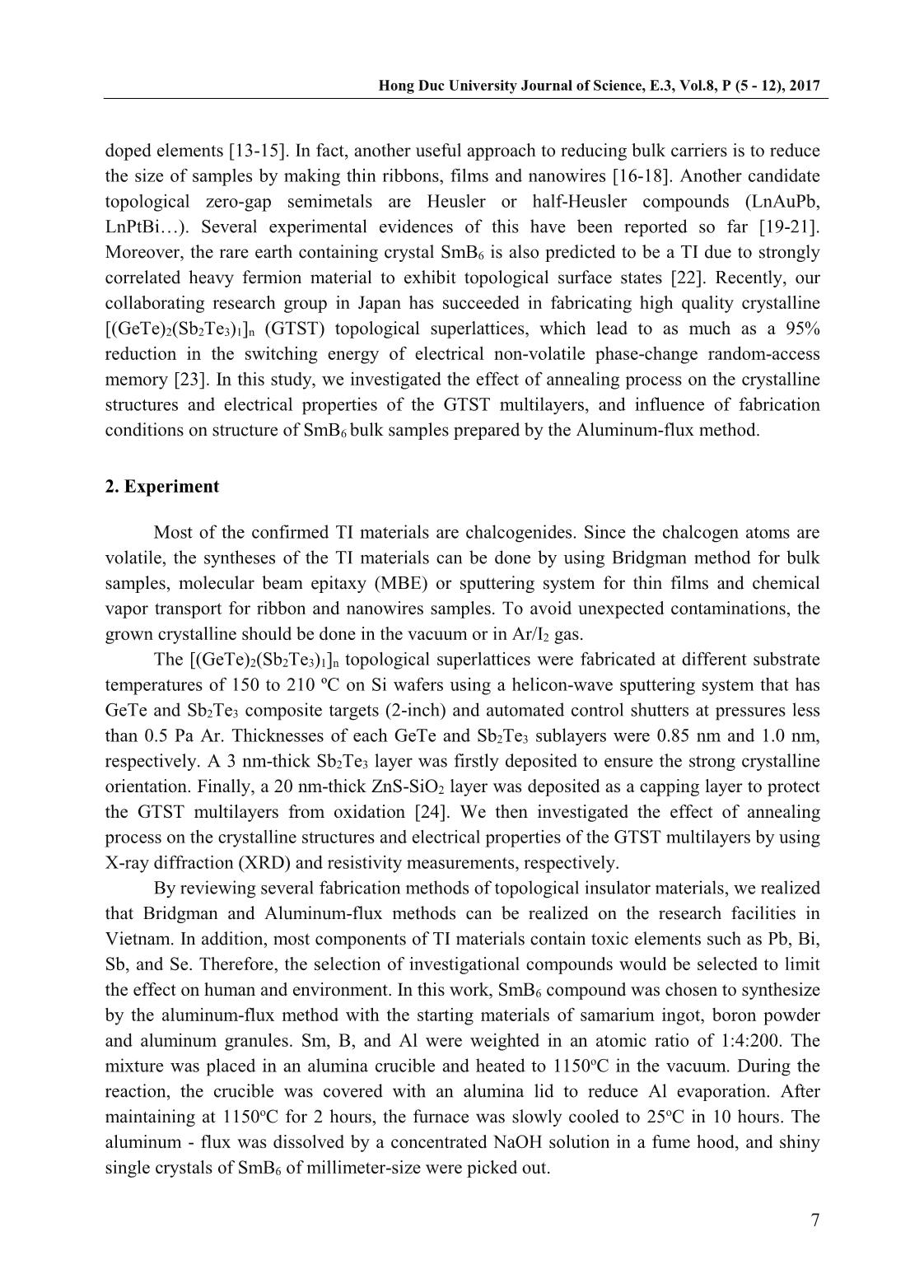
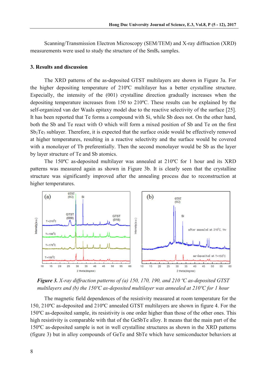
The XRD patterns of the as-deposited GTST multilayers are shown in Figure 3a. For
the higher depositing temperature of 210ºC multilayer has a better crystalline structure.
Especially, the intensity of the (001) crystalline direction gradually increases when the
depositing temperature increases from 150 to 210ºC. These results can be explained by the
self-organized van der Waals epitaxy model due to the reactive selectivity of the surface [25].
It has been reported that Te forms a compound with Si, while Sb does not. On the other hand,
both the Sb and Te react with O which will form a mixed position of Sb and Te on the first
Sb2Te3 sublayer. Therefore, it is expected that the surface oxide would be effectively removed
at higher temperatures, resulting in a reactive selectivity and the surface would be covered
with a monolayer of Tb preferentially. Then the second monolayer would be Sb as the layer
by layer structure of Te and Sb atomics.
The 150ºC as-deposited multilayer was annealed at 210ºC for 1 hour and its XRD
patterns was measured again as shown in Figure 3b. It is clearly seen that the crystalline
structure was significantly improved after the annealing process due to reconstruction at
higher temperatures.
Figure 3. X-ray diffraction patterns of (a) 150, 170, 190, and 210 ºC as-deposited GTST
multilayers and (b) the 150ºC as-deposited multilayer was annealed at 210ºC for 1 hour
The magnetic field dependences of the resistivity measured at room temperature for the
150, 210ºC as-deposited and 210ºC annealed GTST multilayers are shown in figure 4. For the
150ºC as-deposited sample, its resistivity is one order higher than those of the other ones. This
high resistivity is comparable with that of the GeSbTe alloy. It means that the main part of the
150ºC as-deposited sample is not in well crystalline structures as shown in the XRD patterns
(figure 3) but in alloy compounds of GeTe and SbTe which have semiconductor behaviors at
Hong Duc University Journal of Science, E.3, Vol.8, P (5 - 12), 2017
9
room temperature. On the other hand, the resistivity of the 210ºC as-deposited and 210ºC
annealed GTST multilayers is as low as that of a good GeTe-SbTe superlatice. It suggested
that the annealing process at high temperatures can improve the crystalline structure as well as
the electrical property of the low temperature deposited GTST films due to the reconstruction
of atoms.
0
0.01
0.02
0.03
0.04
0.05
-10 -5 0 5 10
150C as-deposited
210C as-deposited
annealed at 210C
R
e
si
st
iv
ity
 (
o
h
m
.c
m
)
Magnetic Field (kOe)
Figure 4. Magnetic field dependences of resistivity for 150ºC as-deposited (opened circles)
and 210ºC as-deposited (opened squares) GTST multilayers, and the 150ºC as-deposited
multilayer was annealed at 210ºC for 1 hour (solid circles)
Figure 5. XRD pattern of SmB6 bulk sample
synthesized at 11500C
Figure 6. SEM image of SmB6 bulk sample
synthesized at 11500C
As shown in [22], the single crystal structure of SmB6 is cubic lattice with constant
a = 4.1353Å. Figure 5 shows XRD pattern of SmB6 prepared at 1150oC using Sm, B, and Al
as raw material. Aluminum here plays the role of reducing the melting temperature of
elements in the component. It can be seen that all the diffraction peaks are not really the
Hong Duc University Journal of Science, E.3, Vol.8, P (5 - 12), 2017
10
SmB6 single crystal structure. However, its XRD patterns are well indexed and assigned to
the parallel crystal planes of (221), (220), (211), (002), (111) [26]. The impurity phases are
identified to be Sm element.
The SEM image is shown in Figure 6. It can be seen that the SmB6 bulk sample
prepared at 1150oC is mainly composed of a great deal of aggregated particles without any
regular shapes, there are some large grains with non-cubic morphology mixing together. In the
next steps, we will continue to synthesize samples at different temperatures to obtain the
better SmB6 single crystals.
4. Conclusion
We investigated the effect of annealing process on the crystalline structures and
electrical properties of the GTST multilayers. It is found that the annealing process at high
temperatures can improve the crystalline structure as well as the electrical property of the low
temperature deposited GTST films due to the reconstruction of atoms. On the other hand, we
also fabricated SmB6 single crystals by the Aluminum-flux method and investigated their
structure. The results showed that the SmB6 bulk sample prepared at 1150oC is mainly
composed of a great deal of aggregated particles without regular shapes. There are some large
grains with non-cubic morphology mixing together.
ACKNOWLEDGMENTS
This work was supported by the basic project of Hong Duc university under grant
number of ĐT-2016-42. A part of the work was done in the Key Laboratory of Electronic
Materials and Devices, Institute of Materials Science (IMS), Vietnam Academy of Science
and Technology (VAST), Vietnam. We are grateful to Assoc. Prof. Dr. Nguyen Huy Dan
(IMS, VAST, Vietnam) for helpful discussions.
References
[1] D. Hsieh, D. Qian, L. Wray, Y. Xia, Y. S. Hor, R. J. Cava, and M. Z. Hasan (2008),
A topological Dirac insulator in a quantum spin Hall phase, Nature: vol. 452, pp.
970-974,
[2] P. Roushan, J. Seo, C. V. Parker, Y. S. Hor, D. Hsieh, D. Qian, A. Richardella, M. Z.
Hasan, R. J. Cava, and Yazdani (2009), Topological surface states protected from
backscattering by chiral spin texture, Nature, vol. 460, pp. 1106-1109.
[3] A. Nishide, A. A. Taskin, Y. Takeichi, T. Okuda, A. Kakizaki, T. Hirahara, K.
Nakatsuji, F. Komori, Y. Ando, amd I. Matsuda (2010), Direct mapping of the spin-
filtered surface bands of a three-dimensional quantum spin Hall insulator, Phys. Rev.
B, vol. 81, 041309(R).
Hong Duc University Journal of Science, E.3, Vol.8, P (5 - 12), 2017
11
[4] H. Zhang, C.-X. Liu, X.-L. Qi, X. Dai, Z. Fang, and S.-C. Zhang (2009), Topological
insulators in Bi, Nature Phys. vol. 5, pp. 438-442.
[5] C.-X. Liu, X.-L. Qi, H. Zhang, X. Dai, Z. Fang, and S.-C. Zhang (2010), Model
Hamitonian for topological insulators, Phys. Rev. B, vol. 82, 045122, 2010.
[6] Y. Xia, D. Qian, D. Hsieh, L. Wray, A. Pal, H. Lin, A. Bansil, D. Grauer, Y. S. Hor, R.
J. Cava, and M. Z. Hasan (2009), Observation of a large-gap topological-insulator
class with a single Dirac cone on the surface, Nature Phys., vol. 5, pp. 398-402.
[7] Y. L. Chen, J. G. Analytis, J.-H. Chu, Z. K. Liu, S.-K. Mo, X. L. Qi, H. J. Zhang, D. H.
Lu, X. Dai, Z. Fang, S. C. Zhang, I. R. Fisher, Z. Hussain, and Z.-X. Shen (2009),
Experimetal realization of a three-dimentional topological insulator, Bi2Te3, Science,
vol. 325, pp. 178-181.
[8] D. Hsieh, Y. Xia, D. Qian, L. Wray, F. Meier, J. H. Dil, J. Osterwalder, L. Patthey, A.
V. Fedorov, H. Lin, A. Bansil, D. Grauer, Y. S. Hor, R. J. Cava, and M. Z. Hasan
(2009), Observation of time-reversal-protected single-Dirac-cone topological-insulator
states in Bi2Te3 and Sb2Te3, Phys. Rev. Lett., vol. 103, 146-401.
[9] Y. Jiang, Y. Wang, M. Chen, Z. Li, C. Song, K. He, L. Wang, X. Chen, X. Ma, and Q.
K. Xue (2012), Landau quantization and the thickness limit of topological insulator
thin films of Sb2Te3, Phys. Rev. Lett., vol. 108, 016401.
[10] C. H. Li et al. (2014), Electrical detection of charge-current-induced spin polarization
due to spin-momentum locking in Bi2Se3, Nature Nanotech., vol. 9, pp. 218-224.
[11] Z. Ren, A. A. Taskin, S. Sasaki, K. Segawa, and Y. Ando (2010), Large bulk resistivity
and surface quantum osillations in the topological insulator Bi2Te2Se, Phys. Rev. B,
vol. 82, 241306(R).
[12] J. Xiong, A. C. Petersen, D. Qu, Y. S. Hor, R. J. Cava, and N. P. Ong (2012), Quantum
oscillations in a topological insulator Bi2Te2Se with large bulk resistivity, Physica E,
vol. 44, pp. 917-920.
[13] Z. Ren, A. A. Taskin, S. Sasaki, K. Segawa, and Y. Ando (2011), Observations of two-
dimensional quantum oscillation and ambipolar transport in the topological insulator
Bi2Se3 achieved by Cd doping, Phys. Rev. B, vol. 84, 075316.
[14] H. Ji, J. M. Allred, M. K. Fuccillo, M. E. Charles, M. Neupane, L. A. Wray, M. Z.
Hasan, and R. J. Cava (2012), A topological insulator in the tetradymite family, Phys.
Rev. B, vol. 85, 201103.
[15] P. Gehring, H.M.Benia, Y.Weng, R. Dinnebier, C. R. Ast, M.Burghard, and K. Kern
(2013), A natural topological insulator, Nano Lett., vol. 13, 1179.
[16] D. Kong, J. C. Randel, H. Peng, J. J. Cha, S. Meister, K. Lai, Y. Chen, Z.-X. Shen, H.
C. Manoharan, and Y. Cui (2010), Topological insulator nanowires and nanoribbons,
Nano Lett., vol. 10, pp. 329-333.
[17] D. Kong, Y. Chen, J. J. Cha, Q. Zhang, J. G. Analytis, K. Lai, Z. Liu, S. S. Hong, K. J.
Koski, S.-K. Mo, Z. Hussain, I. R. Fisher, Z.-X. Shen, and Y. Cui (2011), Ambipolar
field effect in topological insulator nanoplates of (BixSb1-x)2Te3, Nature Nanotechnol.,
vol. 6, pp. 705-709.
Hong Duc University Journal of Science, E.3, Vol.8, P (5 - 12), 2017
12
[18] S. S. Hong, J. J. Cha, D. Kong, and Y. Cui (2012), Ultra-low carrier concentration and
surface-dominant transport in antimony-doped Bi2Se3 topological insulator
nanoribbons, Nature Commun., vol. 3, pp. 757-763.
[19] S. Chadov, X.-L. Qi, J.K¨ubler, G. H. Fecher, C. Felser, and S.-C. Zhang (2010),
Tunable multifunctional topological insulators in ternary Heusler compounds, Nature
Mater, vol. 9, pp. 541-545.
[20] H. Lin, L. A. Wray, Y. Xia, S. Xu, S. Jia, R. J. Cava, A. Bansil, and M. Z. Hasan
(2010), Half-Heusler ternary compounds as new multifunctional experimental
platforms for topological quantum phenomena, Nature Mater., vol. 9, 546-549.
[21] D. Xiao, Y. Yao, W. Feng, J. Wen, W. Zhu, X.-Q. Chen, G. M. Stocks, and Z. Zhang
(2010), Half-Heusler compounds as a new class of three dimensional topological
insulators, Phys. Rev. Lett., vol. 105, 096404.
[22] M. Ciomaga Hatnean, M. R. Lees, D. McK. Paul & G. Balakrishnan (2013), Large,
high quality single-crystals of the new Topological Kondo Insulator, SmB6, Nat. Sci.
Rep., vol.3, 3071, 2013.
[23] Tominaga J et al. (2015), Giant multiferroic effects in topological GeTe-Sb2Te3
superlattices, Sci. Technol. Adv. Master, vol. 16, 014402.
[24] D. Bang et al. (2014), Mirror-symmetric Magneto-optical Kerr Rotation using Visible
Light in [(GeTe)2(Sb2Te3)1]n Topological Superlattices, Nat. Sci. Rep., vol. 4, 5727;
DOI:10.1038/srep05727.
[25] Y. Saito et al. (2015), Self-organized van der Waals epitaxy of layered chalcogenide
structures, Phys. Status Solidi B,vol. 252, 2151-2158.
[26] Lihong Bao et al. (2015), SmB6 nanoparticals: Synthesis, valence states, and magnetic
properties, Journal of Alloys and Compounds, vol. 651, pp. 19-23.
File đính kèm:
 preliminary_study_on_gete_sbte_and_sm_b_topological_insulato.pdf

