Nghiên cứu ảnh hưởng của diện tích bề mặt dẫn điện và các lỗi xếp chồng đến đặc tính của điốt pin 4H-Sic
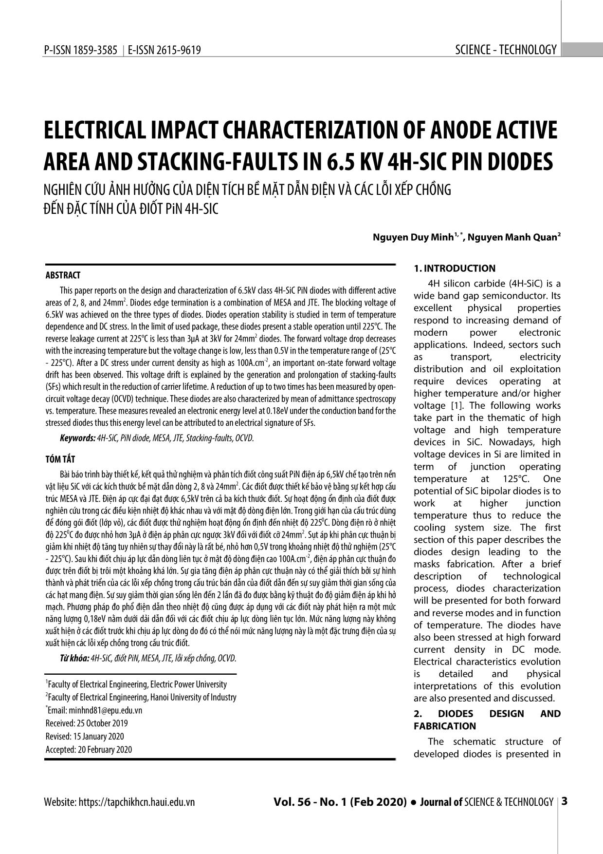
Bài báo trình bày thiết kế, kết quả thử nghiệm và phân tích điốt công suất PiN điện áp 6,5kV chế tạo trên nền
vật liệu SiC với các kích thước bề mặt dẫn dòng 2, 8 và 24mm2. Các điốt được thiết kế bảo vệ bằng sự kết hợp cấu
trúc MESA và JTE. Điện áp cực đại đạt được 6,5kV trên cả ba kích thước điốt. Sự hoạt động ổn định của điốt được
nghiên cứu trong các điều kiện nhiệt độ khác nhau và với mật độ dòng điện lớn. Trong giới hạn của cấu trúc dùng
để đóng gói điốt (lớp vỏ), các điốt được thử nghiệm hoạt động ổn định đến nhiệt độ 2250C. Dòng điện rò ở nhiệt
độ 2250C đo được nhỏ hơn 3µA ở điện áp phân cực ngược 3kV đối với điốt cỡ 24mm2. Sụt áp khi phân cực thuận bị
giảm khi nhiệt độ tăng tuy nhiên sự thay đổi này là rất bé, nhỏ hơn 0,5V trong khoảng nhiệt độ thử nghiệm (25°C
- 225°C). Sau khi điốt chịu áp lực dẫn dòng liên tục ở mật độ dòng điện cao 100A.cm-2, điện áp phân cực thuận đo
được trên điốt bị trôi một khoảng khá lớn. Sự gia tăng điện áp phân cực thuận này có thể giải thích bởi sự hình
thành và phát triển của các lỗi xếp chồng trong cấu trúc bán dẫn của điốt dẫn đến sự suy giảm thời gian sống của
các hạt mang điện. Sự suy giảm thời gian sống lên đến 2 lần đã đo được bằng kỹ thuật đo độ giảm điện áp khi hở
mạch. Phương pháp đo phổ điện dẫn theo nhiệt độ cũng được áp dụng với các điốt này phát hiện ra một mức
năng lượng 0,18eV nằm dưới dải dẫn đối với các điốt chịu áp lực dòng liên tục lớn. Mức năng lượng này không
xuất hiện ở các điốt trước khi chịu áp lực dòng do đó có thể nói mức năng lượng này là một đặc trưng điện của sự
xuất hiện các lỗi xếp chồng trong cấu trúc điốt.
Trang 1
Trang 2
Trang 3
Trang 4
Trang 5
Trang 6
Tóm tắt nội dung tài liệu: Nghiên cứu ảnh hưởng của diện tích bề mặt dẫn điện và các lỗi xếp chồng đến đặc tính của điốt pin 4H-Sic
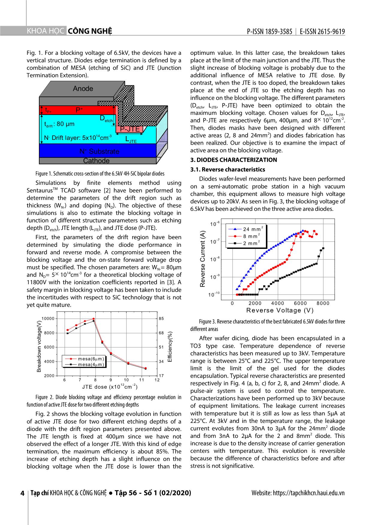
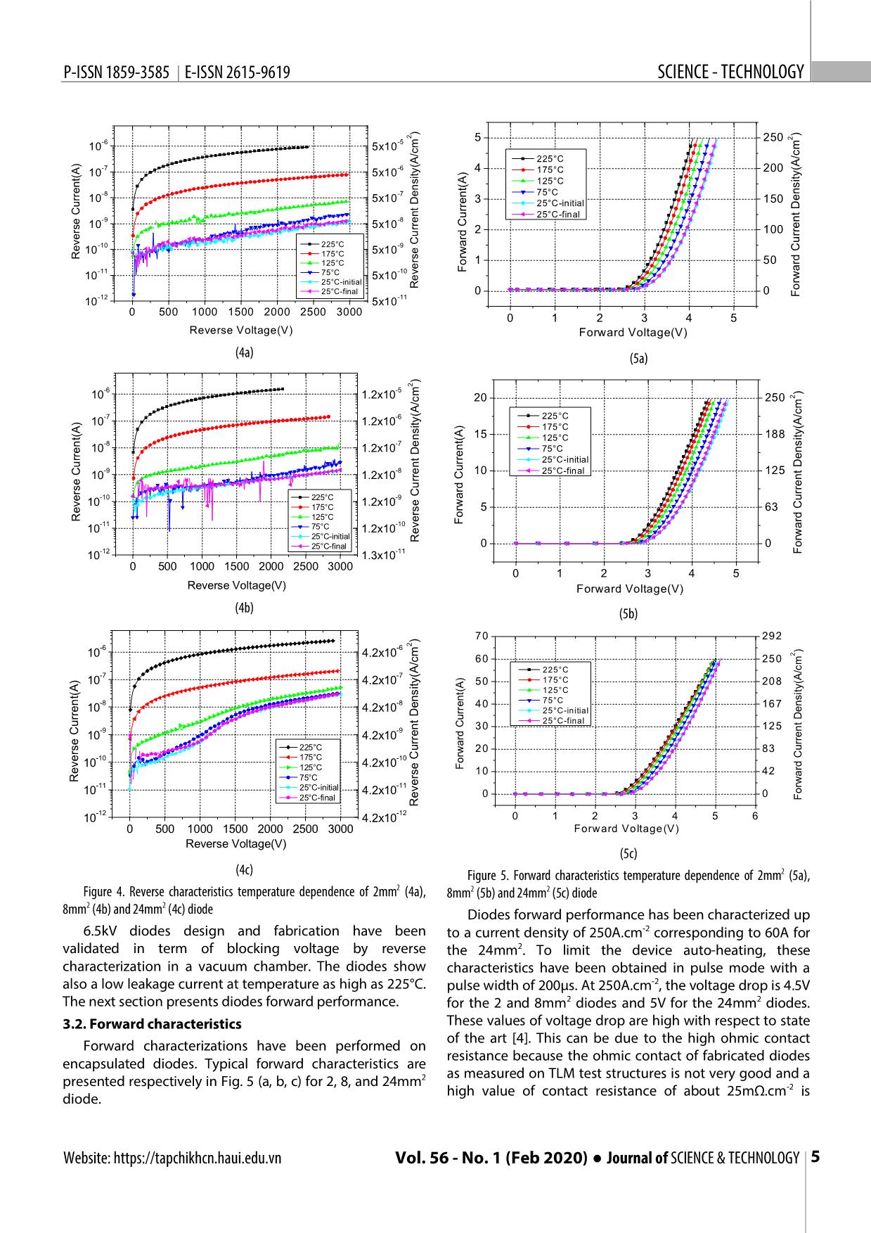
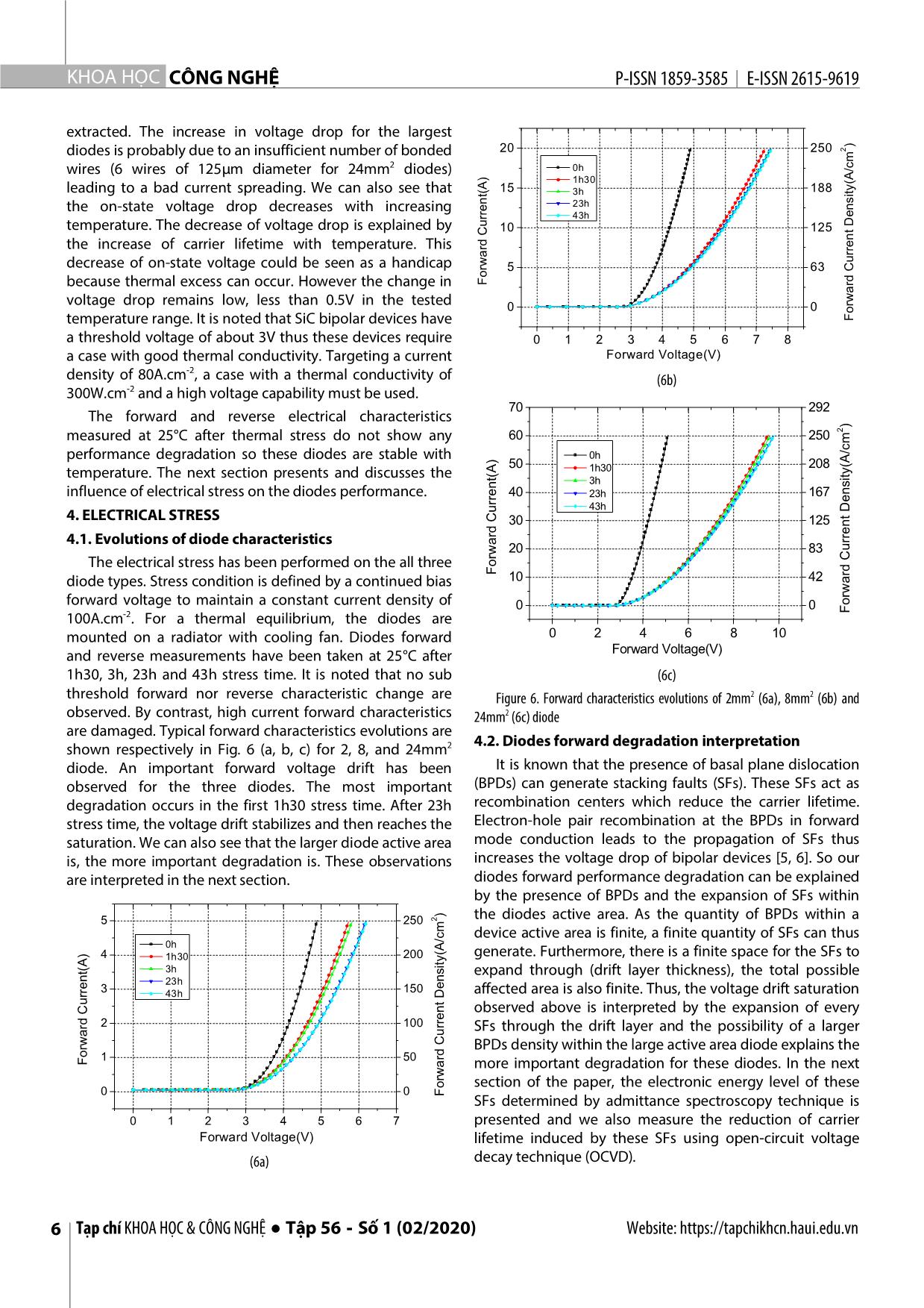
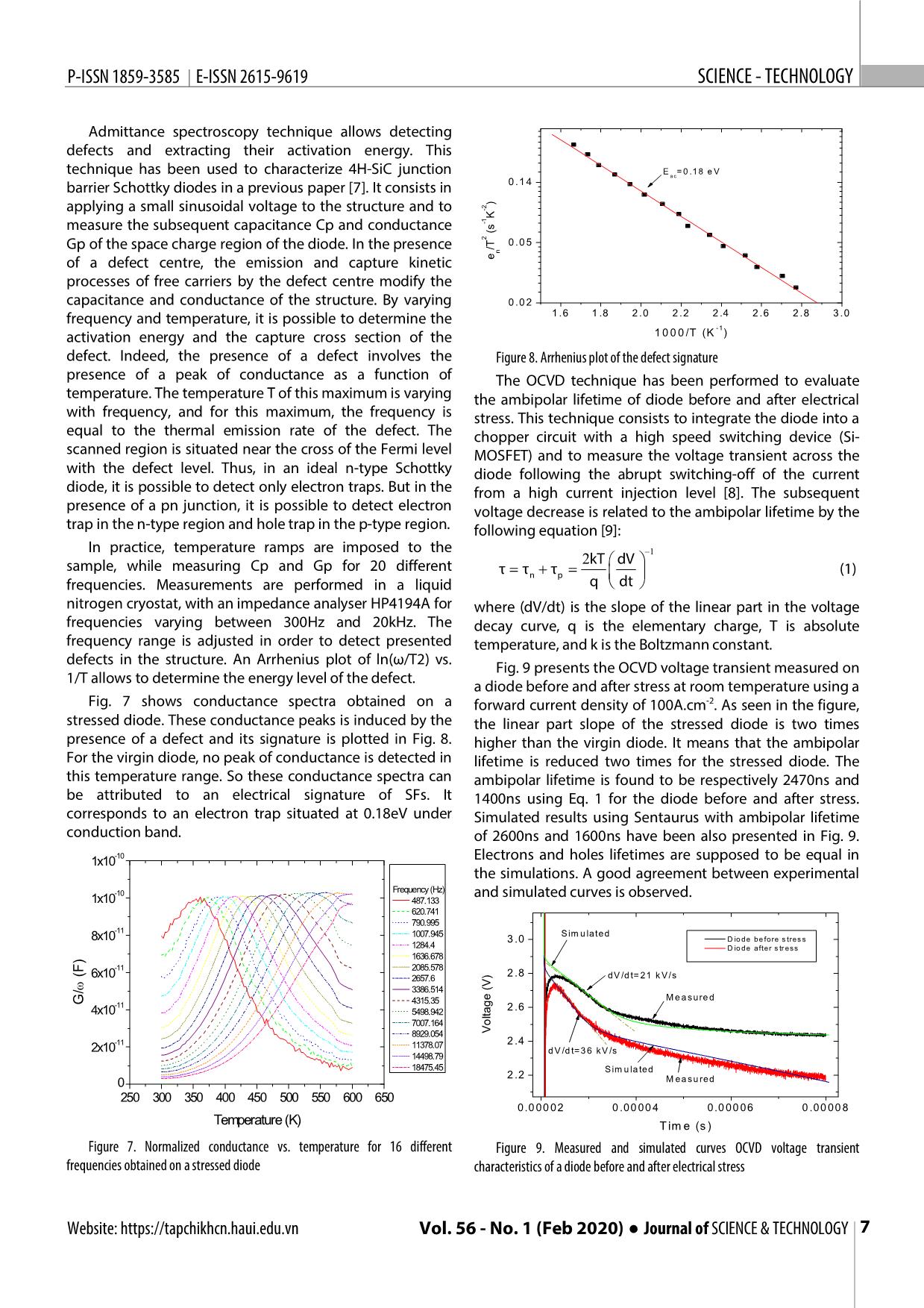
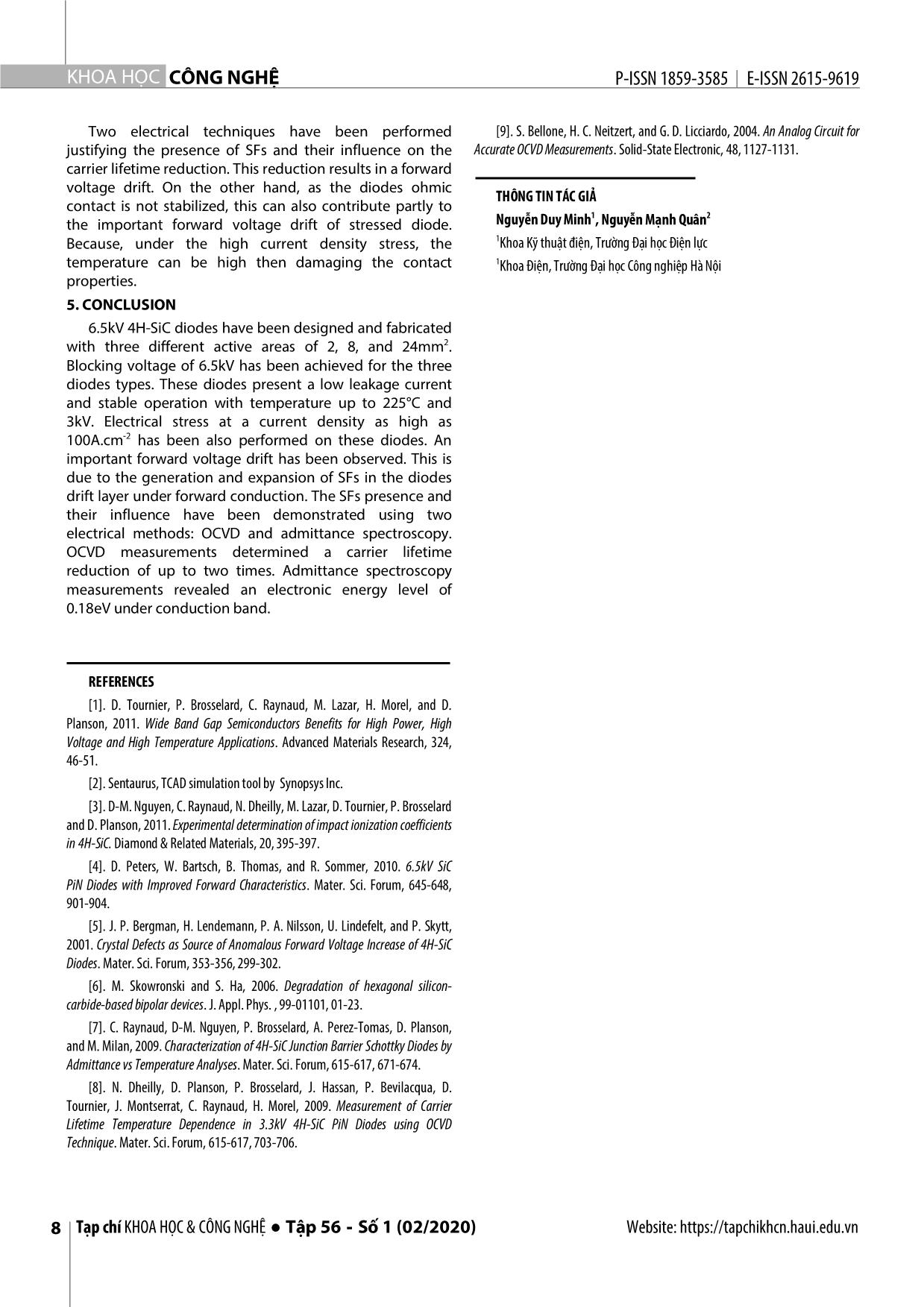
Reverse Voltage(V) Forward Voltage(V) (4a) (5a) ) 2 -6 -5 ) 10 1.2x10 20 250 2 -7 -6 225°C 10 1.2x10 175°C 15 125°C 188 -8 -7 10 1.2x10 75°C 25°C-initial 10-9 1.2x10⁻⁸ 10 25°C-final 125 10-10 225°C 1.2x10⁻⁹ 175°C 5 63 125°C Reverse Current(A) 10-11 75°C 1.2x10⁻¹⁰ Forward Current(A) 25°C-initial Reverse Current Density(A/cm 25°C-final 0 0 10-12 1.3x10⁻¹¹ Forward Current Density(A/cm 0 500 1000 1500 2000 2500 3000 0 1 2 3 4 5 Reverse Voltage(V) Forward Voltage(V) (4b) (5b) 70 292 ) -6 -6 2 ) 10 4.2x10 2 60 250 225°C -7 -7 10 4.2x10 50 175°C 208 125°C -8 -8 40 75°C 167 10 4.2x10 25°C-initial 25°C-final 30 125 10-9 4.2x10⁻⁹ 225°C 20 83 10-10 175°C 4.2x10⁻¹⁰ 125°C Forward Current(A) 10 42 Reverse Current(A) 75°C -11 25°C-initial -11 10 4.2x10 0 0 25°C-final Forward Current Density(A/cm Reverse Current Density(A/cm 10-12 4.2x10⁻¹² 0 1 2 3 4 5 6 Forward Voltage(V) 0 500 1000 1500 2000 2500 3000 Reverse Voltage(V) (5c) (4c) Figure 5. Forward characteristics temperature dependence of 2mm2 (5a), Figure 4. Reverse characteristics temperature dependence of 2mm2 (4a), 8mm2 (5b) and 24mm2 (5c) diode 2 2 8mm (4b) and 24mm (4c) diode Diodes forward performance has been characterized up 6.5kV diodes design and fabrication have been to a current density of 250A.cm-2 corresponding to 60A for validated in term of blocking voltage by reverse the 24mm2. To limit the device auto-heating, these characterization in a vacuum chamber. The diodes show characteristics have been obtained in pulse mode with a also a low leakage current at temperature as high as 225°C. pulse width of 200µs. At 250A.cm-2, the voltage drop is 4.5V The next section presents diodes forward performance. for the 2 and 8mm2 diodes and 5V for the 24mm2 diodes. 3.2. Forward characteristics These values of voltage drop are high with respect to state of the art [4]. This can be due to the high ohmic contact Forward characterizations have been performed on resistance because the ohmic contact of fabricated diodes encapsulated diodes. Typical forward characteristics are as measured on TLM test structures is not very good and a presented respectively in Fig. 5 (a, b, c) for 2, 8, and 24mm2 high value of contact resistance of about 25mΩ.cm-2 is diode. Website: https://tapchikhcn.haui.edu.vn Vol. 56 - No. 1 (Feb 2020) ● Journal of SCIENCE & TECHNOLOGY 5 KHOA H ỌC CÔNG NGHỆ P - ISSN 1859 - 3585 E - ISSN 2615 - 961 9 extracted. The increase in voltage drop for the largest ) diodes is probably due to an insufficient number of bonded 20 250 2 wires (6 wires of 125µm diameter for 24mm2 diodes) 0h 1h30 leading to a bad current spreading. We can also see that 15 3h 188 the on-state voltage drop decreases with increasing 23h 43h temperature. The decrease of voltage drop is explained by 10 125 the increase of carrier lifetime with temperature. This decrease of on-state voltage could be seen as a handicap 5 63 because thermal excess can occur. However the change in Forward Current(A) voltage drop remains low, less than 0.5V in the tested 0 0 temperature range. It is noted that SiC bipolar devices have Forward CurrentDensity(A/cm a threshold voltage of about 3V thus these devices require 0 1 2 3 4 5 6 7 8 a case with good thermal conductivity. Targeting a current Forward Voltage(V) -2 density of 80A.cm , a case with a thermal conductivity of (6b) 300W.cm-2 and a high voltage capability must be used. 70 292 The forward and reverse electrical characteristics ) measured at 25°C after thermal stress do not show any 60 250 2 performance degradation so these diodes are stable with 0h 50 1h30 208 temperature. The next section presents and discusses the 3h influence of electrical stress on the diodes performance. 40 23h 167 43h 4. ELECTRICAL STRESS 30 125 4.1. Evolutions of diode characteristics 20 83 The electrical stress has been performed on the all three diode types. Stress condition is defined by a continued bias Forward Current(A) 10 42 forward voltage to maintain a constant current density of 0 0 100A.cm-2. For a thermal equilibrium, the diodes are Forward Current Density(A/cm mounted on a radiator with cooling fan. Diodes forward 0 2 4 6 8 10 and reverse measurements have been taken at 25°C after Forward Voltage(V) 1h30, 3h, 23h and 43h stress time. It is noted that no sub (6c) threshold forward nor reverse characteristic change are Figure 6. Forward characteristics evolutions of 2mm2 (6a), 8mm2 (6b) and observed. By contrast, high current forward characteristics 24mm2 (6c) diode are damaged. Typical forward characteristics evolutions are 4.2. Diodes forward degradation interpretation shown respectively in Fig. 6 (a, b, c) for 2, 8, and 24mm2 diode. An important forward voltage drift has been It is known that the presence of basal plane dislocation observed for the three diodes. The most important (BPDs) can generate stacking faults (SFs). These SFs act as degradation occurs in the first 1h30 stress time. After 23h recombination centers which reduce the carrier lifetime. stress time, the voltage drift stabilizes and then reaches the Electron-hole pair recombination at the BPDs in forward saturation. We can also see that the larger diode active area mode conduction leads to the propagation of SFs thus is, the more important degradation is. These observations increases the voltage drop of bipolar devices [5, 6]. So our are interpreted in the next section. diodes forward performance degradation can be explained by the presence of BPDs and the expansion of SFs within ) 5 250 2 the diodes active area. As the quantity of BPDs within a device active area is finite, a finite quantity of SFs can thus 0h 4 1h30 200 generate. Furthermore, there is a finite space for the SFs to 3h expand through (drift layer thickness), the total possible 23h 3 43h 150 affected area is also finite. Thus, the voltage drift saturation observed above is interpreted by the expansion of every 2 100 SFs through the drift layer and the possibility of a larger BPDs density within the large active area diode explains the 1 50 Forward Current(A)Forward more important degradation for these diodes. In the next section of the paper, the electronic energy level of these 0 0 Forward Current Density(A/cm SFs determined by admittance spectroscopy technique is 0 1 2 3 4 5 6 7 presented and we also measure the reduction of carrier Forward Voltage(V) lifetime induced by these SFs using open-circuit voltage (6a) decay technique (OCVD). 6 Tạp chí KHOA HỌC & CÔNG NGHỆ ● Tập 56 - Số 1 (02/2020) Website: https://tapchikhcn.haui.edu.vn P-ISSN 1859-3585 E-ISSN 2615-9619 SCIENCE - TECHNOLOGY Admittance spectroscopy technique allows detecting defects and extracting their activation energy. This E = 0 .1 8 e V technique has been used to characterize 4H-SiC junction a c barrier Schottky diodes in a previous paper [7]. It consists in 0 .1 4 ) applying a small sinusoidal voltage to the structure and to -2 K measure the subsequent capacitance Cp and conductance -1 (s 2 0 .0 5 Gp of the space charge region of the diode. In the presence /T n of a defect centre, the emission and capture kinetic e processes of free carriers by the defect centre modify the capacitance and conductance of the structure. By varying 0 .0 2 frequency and temperature, it is possible to determine the 1.6 1.8 2.0 2.2 2.4 2.6 2.8 3.0 -1 activation energy and the capture cross section of the 1 0 0 0 /T (K ) defect. Indeed, the presence of a defect involves the Figure 8. Arrhenius plot of the defect signature presence of a peak of conductance as a function of The OCVD technique has been performed to evaluate temperature. The temperature T of this maximum is varying the ambipolar lifetime of diode before and after electrical with frequency, and for this maximum, the frequency is stress. This technique consists to integrate the diode into a equal to the thermal emission rate of the defect. The chopper circuit with a high speed switching device (Si- scanned region is situated near the cross of the Fermi level MOSFET) and to measure the voltage transient across the with the defect level. Thus, in an ideal n-type Schottky diode following the abrupt switching-off of the current diode, it is possible to detect only electron traps. But in the from a high current injection level [8]. The subsequent presence of a pn junction, it is possible to detect electron voltage decrease is related to the ambipolar lifetime by the trap in the n-type region and hole trap in the p-type region. following equation [9]: In practice, temperature ramps are imposed to the 1 sample, while measuring Cp and Gp for 20 different 2kT dV τ τn τ p (1) frequencies. Measurements are performed in a liquid q dt nitrogen cryostat, with an impedance analyser HP4194A for where (dV/dt) is the slope of the linear part in the voltage frequencies varying between 300Hz and 20kHz. The decay curve, q is the elementary charge, T is absolute frequency range is adjusted in order to detect presented temperature, and k is the Boltzmann constant. defects in the structure. An Arrhenius plot of ln(ω/T2) vs. Fig. 9 presents the OCVD voltage transient measured on 1/T allows to determine the energy level of the defect. a diode before and after stress at room temperature using a Fig. 7 shows conductance spectra obtained on a forward current density of 100A.cm-2. As seen in the figure, stressed diode. These conductance peaks is induced by the the linear part slope of the stressed diode is two times presence of a defect and its signature is plotted in Fig. 8. higher than the virgin diode. It means that the ambipolar For the virgin diode, no peak of conductance is detected in lifetime is reduced two times for the stressed diode. The this temperature range. So these conductance spectra can ambipolar lifetime is found to be respectively 2470ns and be attributed to an electrical signature of SFs. It 1400ns using Eq. 1 for the diode before and after stress. corresponds to an electron trap situated at 0.18eV under Simulated results using Sentaurus with ambipolar lifetime conduction band. of 2600ns and 1600ns have been also presented in Fig. 9. 1x10⁻¹⁰ Electrons and holes lifetimes are supposed to be equal in the simulations. A good agreement between experimental -10 Frequency (Hz) and simulated curves is observed. 1x10 487.133 620.741 790.995 -11 1007.945 Sim u lated 8x10 3 .0 D io de be fore s tres s 1284.4 D io de after s tr ess 1636.678 -11 2085.578 6x10 2 .8 dV/dt=21 kV/s (F) 2657.6 3386.514 M e a sure d G/ -11 4315.35 4x10 5498.942 2 .6 7007.164 8929.054 Voltage (V) -11 11378.07 2 .4 2x10 dV/dt=36 kV/s 14498.79 18475.45 Sim u la ted 2 .2 0 M ea su red 250 300 350 400 450 500 550 600 650 0.00002 0.00004 0.00006 0.00008 Temperature (K) T im e (s ) Figure 7. Normalized conductance vs. temperature for 16 different Figure 9. Measured and simulated curves OCVD voltage transient frequencies obtained on a stressed diode characteristics of a diode before and after electrical stress Website: https://tapchikhcn.haui.edu.vn Vol. 56 - No. 1 (Feb 2020) ● Journal of SCIENCE & TECHNOLOGY 7 KHOA H ỌC CÔNG NGHỆ P - ISSN 1859 - 3585 E - ISSN 2615 - 961 9 Two electrical techniques have been performed [9]. S. Bellone, H. C. Neitzert, and G. D. Licciardo, 2004. An Analog Circuit for justifying the presence of SFs and their influence on the Accurate OCVD Measurements. Solid-State Electronic, 48, 1127-1131. carrier lifetime reduction. This reduction results in a forward voltage drift. On the other hand, as the diodes ohmic THÔNG TIN TÁC GIẢ contact is not stabilized, this can also contribute partly to 1 2 the important forward voltage drift of stressed diode. Nguyễn Duy Minh , Nguyễn Mạnh Quân Because, under the high current density stress, the 1Khoa Kỹ thuật điện, Trường Đại học Điện lực temperature can be high then damaging the contact 1Khoa Điện, Trường Đại học Công nghiệp Hà Nội properties. 5. CONCLUSION 6.5kV 4H-SiC diodes have been designed and fabricated with three different active areas of 2, 8, and 24mm2. Blocking voltage of 6.5kV has been achieved for the three diodes types. These diodes present a low leakage current and stable operation with temperature up to 225°C and 3kV. Electrical stress at a current density as high as 100A.cm-2 has been also performed on these diodes. An important forward voltage drift has been observed. This is due to the generation and expansion of SFs in the diodes drift layer under forward conduction. The SFs presence and their influence have been demonstrated using two electrical methods: OCVD and admittance spectroscopy. OCVD measurements determined a carrier lifetime reduction of up to two times. Admittance spectroscopy measurements revealed an electronic energy level of 0.18eV under conduction band. REFERENCES [1]. D. Tournier, P. Brosselard, C. Raynaud, M. Lazar, H. Morel, and D. Planson, 2011. Wide Band Gap Semiconductors Benefits for High Power, High Voltage and High Temperature Applications. Advanced Materials Research, 324, 46-51. [2]. Sentaurus, TCAD simulation tool by Synopsys Inc. [3]. D-M. Nguyen, C. Raynaud, N. Dheilly, M. Lazar, D. Tournier, P. Brosselard and D. Planson, 2011. Experimental determination of impact ionization coefficients in 4H-SiC. Diamond & Related Materials, 20, 395-397. [4]. D. Peters, W. Bartsch, B. Thomas, and R. Sommer, 2010. 6.5kV SiC PiN Diodes with Improved Forward Characteristics. Mater. Sci. Forum, 645-648, 901-904. [5]. J. P. Bergman, H. Lendemann, P. A. Nilsson, U. Lindefelt, and P. Skytt, 2001. Crystal Defects as Source of Anomalous Forward Voltage Increase of 4H-SiC Diodes. Mater. Sci. Forum, 353-356, 299-302. [6]. M. Skowronski and S. Ha, 2006. Degradation of hexagonal silicon- carbide-based bipolar devices. J. Appl. Phys. , 99-01101, 01-23. [7]. C. Raynaud, D-M. Nguyen, P. Brosselard, A. Perez-Tomas, D. Planson, and M. Milan, 2009. Characterization of 4H-SiC Junction Barrier Schottky Diodes by Admittance vs Temperature Analyses. Mater. Sci. Forum, 615-617, 671-674. [8]. N. Dheilly, D. Planson, P. Brosselard, J. Hassan, P. Bevilacqua, D. Tournier, J. Montserrat, C. Raynaud, H. Morel, 2009. Measurement of Carrier Lifetime Temperature Dependence in 3.3kV 4H-SiC PiN Diodes using OCVD Technique. Mater. Sci. Forum, 615-617, 703-706. 8 Tạp chí KHOA HỌC & CÔNG NGHỆ ● Tập 56 - Số 1 (02/2020) Website: https://tapchikhcn.haui.edu.vn
File đính kèm:
 nghien_cuu_anh_huong_cua_dien_tich_be_mat_dan_dien_va_cac_lo.pdf

