Hardware trojan detection technique using frequency characteristic analysis of path delay in application specific integrated circuits
Từ thập niên 2010, Trojan phần
cứng (HT) đã trở thành một vấn đề nghiêm
trọng đối với bảo mật phần cứng, do xu hướng
thuê sản xuất mạch tích hợp (Integrated
Circuit - IC). Khi quá trình chế tạo IC trở nên
phức tạp và tốn kém, ngày càng nhiều nhà sản
xuất chip lựa chọn phương án thuê lại một
phần hoặc toàn bộ thiết kế IC. Xu hướng này
tạo ra lỗ hổng trong bảo mật phần cứng, vì
một công ty không đáng tin cậy có thể thực
hiện các sửa đổi độc hại vào trong mạch
nguyên bản ở giai đoạn thiết kế hoặc chế tạo.
Do đó, đánh giá rủi ro và đề xuất giải pháp
phát hiện HT là một trong những nhiệm vụ
hết sức quan trọng. Bài báo này trình bày một
giải pháp phát hiện HT sử dụng phân tích đặc
tính tần số của độ trễ đường truyền tín hiệu.
Kết quả cho thấy, thực hiện khảo sát với bước
tần số 0,016 MHz có thể phát hiện được HT có
kích thước 0,2% so với thiết kế ban đầu.
Trang 1
Trang 2
Trang 3
Trang 4
Trang 5
Trang 6
Trang 7
Trang 8
Tóm tắt nội dung tài liệu: Hardware trojan detection technique using frequency characteristic analysis of path delay in application specific integrated circuits
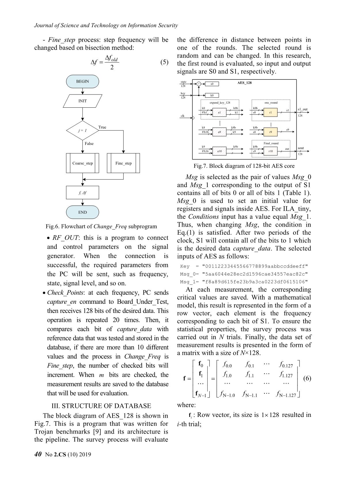
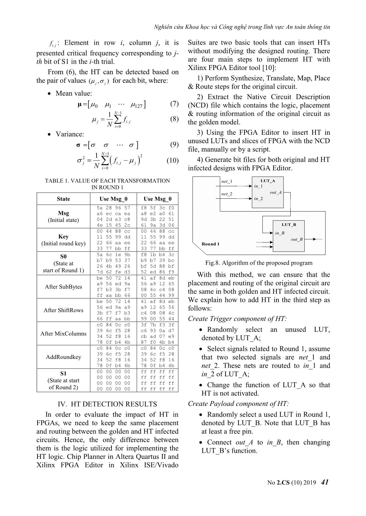
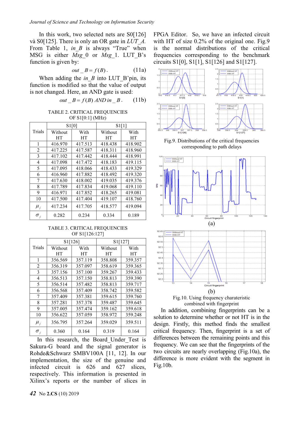
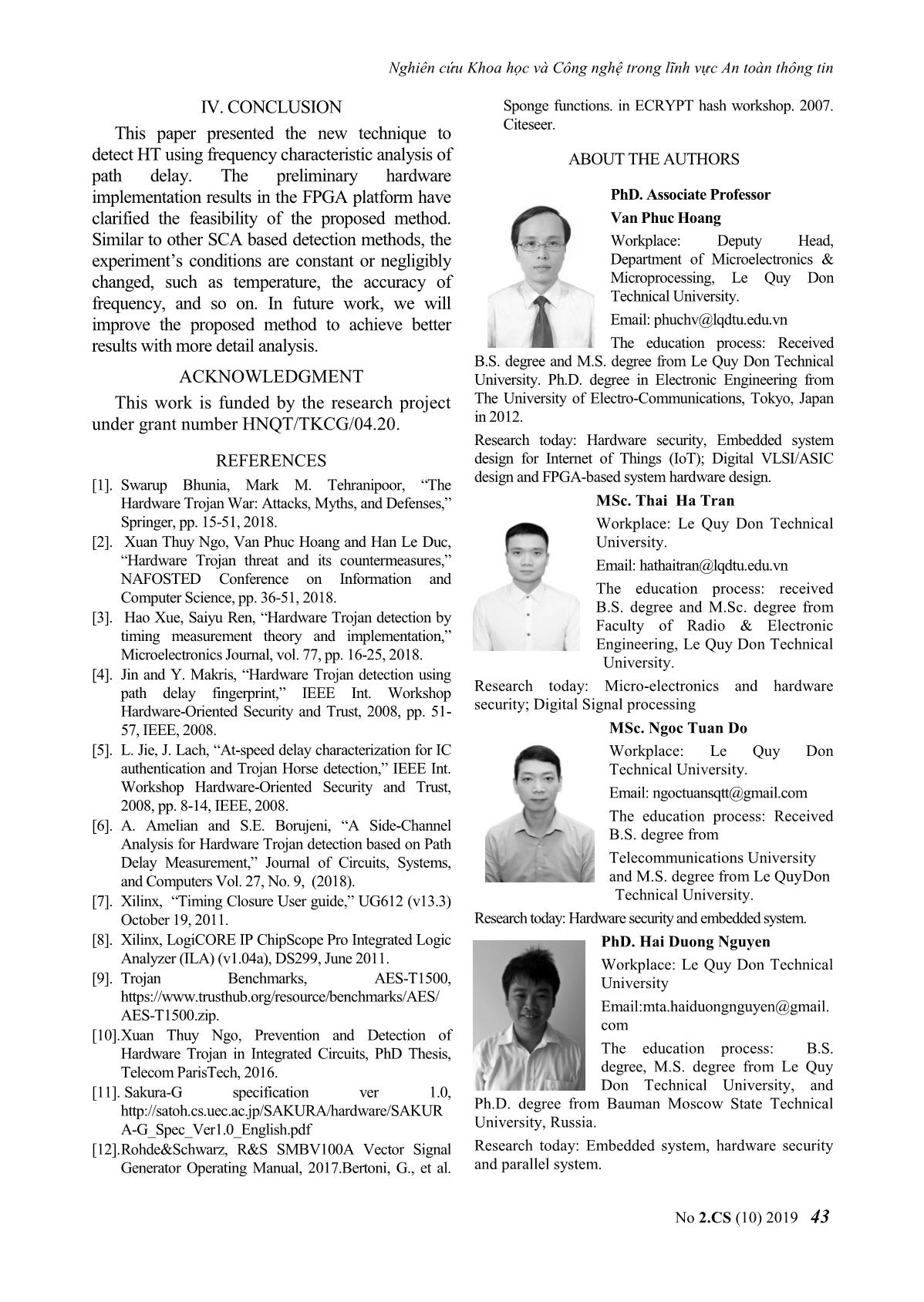
Key_AES BEGIN UART_interface 128 Msg_AES AES_128 UART_RX (MainDesign) 128 RX_DV m, Δf = Δf0 Cipher_AES RX_DV INIT RX_Byte rx_in f=f0 , i = 0 128 RX_Byte RX_Serial Conditions ext _ clk clk 128 g_CLKS_PER_BIT TriggerPort Conditions enable UART_control TX_Active UART_TX TX_Active True Capture_done TX_Done i = m ? DataPort TX_Done TX_Byte tx_out 128 ILA_tiny captureData TX_Byte TX_Serial TX_DV False 128 TX_DV clear clk Change_Freq. clk_ext g_CLKS_PER_BIT (result: f, Δf ) ext clk_int clk_int clk_int _ clk RF_OUT Fig.4. Block diagram of the proposed design fout = f C. Algorithm of the proposed program Check_Points Algorithm of the main program is illustrated in (result: i , j) Fig.5, it is divided into three subprograms, where: m : total number of bits (or points) to check, in this research m 128; Save to file i : number of checked bits, default i 0; j : number of bits is being checked, default END j 0; Fig.5. Algorithm of the proposed program f0 : initial frequency; Change_Freq is a subprogram to f0 : maximum of step frequency, default value: change the frequency of signal f0 4.096 MHz; generator, determine the pair of values f : instantaneous frequency; (,)ff . At the previous loop, assuming f : instantaneous step frequency; that the pair values of frequency and its f : minimum of step frequency, default value step are (,)ffold old . Choosing f 0.016 MHz. Coarse_step or Fine_step process will depend on j - the number of bits is being checked. Then, is sent to the next subprogram called RF_OUT. In coarse_step process: + if j 0 : step frequency will get previous value: ff old (2) + if j 0 : the new step value will be less than the old value four times: f f old (3) 4 and f fold f (4) No 2.CS (10) 2019 39 Journal of Science and Technology on Information Security - Fine_step process: step frequency will be the difference in distance between points in changed based on bisection method: one of the rounds. The selected round is random and can be changed. In this research, fold f (5) the first round is evaluated, so input and output 2 signals are S0 and S1, respectively. BEGIN state + s0 AES_128 128 key k0 128 INIT expand_key_128 one_round k0 k0b k0b s1 s1_out 8'h1 a1 k1 s0 r1 clk 128 True k8 k8b k8b s9 j = 1 8'h1b a9 k9 s8 r9 False Final_round k9 k9b k9b out sout 8'h36 a10 s9 r10 128 Coarse_step Fine_step Fig.7. Block diagram of 128-bit AES core Msg is selected as the pair of values Msg_0 and Msg_1 corresponding to the output of S1 f, Δf contains all of bits 0 or all of bits 1 (Table 1). Msg_0 is used to set an initial value for registers and signals inside AES. For ILA_tiny, END the Conditions input has a value equal Msg_1. Fig.6. Flowchart of Change_Freq subprogram Thus, when changing Msg, the condition in Eq.(1) is satisfied. After two periods of the RF_OUT: this is a program to connect clock, S1 will contain all of the bits to 1 which and control parameters on the signal is the desired data capture_data. The selected generator. When the connection is inputs of AES as follows: successful, the required parameters from Key = "00112233445566778899aabbccddeeff" the PC will be sent, such as frequency, Msg_0= "5aa6044e28ec2d1596cae34557eac82c" state, signal level, and so on. Msg_1= "f8a89d615fe23b9a3ca0223df0615106" Check_Points: at each frequency, PC sends At each measurement, the corresponding critical values are saved. With a mathematical capture_en command to Board_Under_Test, model, this result is represented in the form of a then receives 128 bits of the desired data. This row vector, each element is the frequency operation is repeated 20 times. Then, it corresponding to each bit of S1. To ensure the compares each bit of capture_data with statistical properties, the survey process was reference data that was tested and stored in the carried out in N trials. Finally, the data set of database, if there are more than 10 different measurement results is presented in the form of a matrix with a size of N×128. values and the process in Change_Freq is Fine_step, the number of checked bits will f0 f0.0 f 0.1 f 0.127 increment. When m bits are checked, the f1 f1.0 f 1.1 f 1.127 f (6) measurement results are saved to the database that will be used for evaluation. fN 1 fN 1.0 f N 1.1 f N 1.127 III. STRUCTURE OF DATABASE where: The block diagram of AES_128 is shown in fi : Row vector, its size is 1 128 resulted in Fig.7. This is a program that was written for i-th trial; Trojan benchmarks [9] and its architecture is the pipeline. The survey process will evaluate 40 No 2.CS (10) 2019 Nghiên cứu Khoa học và Công nghệ trong lĩnh vực An toàn thông tin fij. : Element in row i, column j, it is Suites are two basic tools that can insert HTs presented critical frequency corresponding to j- without modifying the designed routing. There th bit of S1 in the i-th trial. are four main steps to implement HT with Xilinx FPGA Editor tool [10]: From (6), the HT can be detected based on the pair of values (,) for each bit, where: 1) Perform Synthesize, Translate, Map, Place jj & Route steps for the original circuit. Mean value: 2) Extract the Native Circuit Description μ 0 1 127 (7) (NCD) file which contains the logic, placement 1 N 1 & routing information of the original circuit as f (8) j i. j the golden model. N i 0 Variance: 3) Using the FPGA Editor to insert HT in 2 2 2 2 unused LUTs and slices of FPGA with the NCD σ (9) 0 1 127 file, manually or by a script. N 1 1 2 2 4) Generate bit files for both original and HT j f i. j j (10) N i 0 infected designs with FPGA Editor. TABLE 1. VALUE OF EACH TRANSFORMATION net_1 LUT_A IN ROUND 1 in_1 net_2 out_A State Use Msg_0 Use Msg_0 in_2 5a 28 96 57 f8 5f 3c f0 Msg a6 ec ca ea a8 e2 a0 61 (Initial state) 04 2d e3 c8 9d 3b 22 51 4e 15 45 2c 61 9a 3d 06 LUT_B 00 44 88 cc 00 44 88 cc in_B 11 55 99 dd 11 55 99 dd Key out_B (Initial round key) 22 66 aa ee 22 66 aa ee Round 1 33 77 bb ff 33 77 bb ff S0 5a 6c 1e 9b f8 1b b4 3c b7 b9 53 37 b9 b7 39 bc (State at 26 4b 49 26 bf 5d 88 bf Fig.8. Algorithm of the proposed program start of Round 1) 7d 62 fe d3 52 ed 86 f9 be 50 72 14 41 af 8d eb With this method, we can ensure that the a9 56 ed 9a 56 a9 12 65 placement and routing of the original circuit are After SubBytes f7 b3 3b f7 08 4c c4 08 ff aa bb 66 00 55 44 99 the same in both golden and HT infected circuit. be 50 72 14 41 af 8d eb We explain how to add HT in the third step as 56 ed 9a a9 a9 12 65 56 follows: After ShiftRows 3b f7 f7 b3 c4 08 08 4c 66 ff aa bb 99 00 55 44 Create Trigger component of HT: c0 84 0c c0 3f 7b f3 3f 39 6c f5 28 c6 93 0a d7 Randomly select an unused LUT, After MixColumns 34 52 f8 16 cb ad 07 e9 denoted by LUT_A; 78 0f b4 4b 87 f0 4b b4 c0 84 0c c0 c0 84 0c c0 Select signals related to Round 1, assume 39 6c f5 28 39 6c f5 28 AddRoundkey 34 52 f8 16 34 52 f8 16 that two selected signals are net_1 and 78 0f b4 4b 78 0f b4 4b net_2. These nets are routed to in_1 and S1 00 00 00 00 ff ff ff ff 00 00 00 00 ff ff ff ff in_2 of LUT_A; (State at start 00 00 00 00 ff ff ff ff Change the function of LUT_A so that of Round 2) 00 00 00 00 ff ff ff ff HT is not activated. IV. HT DETECTION RESULTS Create Payload component of HT: In order to evaluate the impact of HT in Randomly select a used LUT in Round 1, FPGAs, we need to keep the same placement denoted by LUT_B. Note that LUT_B has and routing between the golden and HT infected at least a free pin. circuits. Hence, the only difference between Connect out_A to in_B, then changing them is the logic utilized for implementing the LUT_B’s function. HT logic. Chip Planner in Altera Quartus II and Xilinx FPGA Editor in Xilinx ISE/Vivado No 2.CS (10) 2019 41 Journal of Science and Technology on Information Security In this work, two selected nets are S0[126] FPGA Editor. So, we have an infected circuit và S0[125]. There is only an OR gate in LUT_A. with HT of size 0.2% of the original one. Fig.9 From Table 1, in_B is always “True” when is the normal distributions of the critical MSG is either Msg_0 or Msg_1. LUT_B’s frequencies corresponding to the benchmark function is given by: circuits S1[0], S1[1], S1[126] and S1[127]. out_() B f B . (11a) When adding the in_B into LUT_B’pin, its function is modified so that the value of output is not changed. Here, an AND gate is used: out_()_ B f B AND in B . (11b) TABLE 2. CRITICAL FREQUENCIES OF S1[0:1] (MHz) S1[0] S1[1] Trials Without With Without With HT HT HT HT Fig.9. Distributions of the critical frequencies 1 416.970 417.513 418.438 418.902 corresponding to path delays 2 417.225 417.587 418.311 418.960 3 417.102 417.442 418.444 418.991 4 417.098 417.472 418.183 419.115 5 417.095 418.066 418.433 419.329 6 416.960 417.882 418.492 419.320 7 417.630 418.002 419.035 419.376 8 417.789 417.834 419.068 419.110 9 416.971 417.852 418.265 419.081 10 417.500 417.404 419.107 418.760 j 417.234 417.705 418.577 419.094 j 0.282 0.234 0.334 0.189 (a) TABLE 3. CRITICAL FREQUENCIES OF S1[126:127] S1[126] S1[127] Trials Without With Without With HT HT HT HT 1 356.569 357.119 358.808 359.357 2 356.319 357.097 358.619 359.365 3 357.156 357.100 359.267 359.433 4 356.513 357.150 358.813 359.390 5 356.514 357.482 358.813 359.717 6 356.568 357.409 358.742 359.582 (b) 7 357.409 357.381 359.615 359.760 Fig.10. Using frequency charateristic 8 357.281 357.378 359.487 359.645 combined with fingerprint 9 357.005 357.474 359.162 359.618 In addition, combining fingerprints can be a 10 356.622 357.059 358.972 359.248 solution to determine whether or not HT is in the 356.795 357.264 359.029 359.511 design. Firstly, this method finds the smallest 0.360 0.164 0.319 0.164 critical frequency. Then, fingerprint is a set of In this research, the Board_Under_Test is differences between the remaining points and this Sakura-G board and the signal generator is frequency. We can see that the fingerprints of the Rohde&Schwarz SMBV100A [11, 12]. In our two circuits are nearly overlapping (Fig.10a), the implementation, the size of the genuine and difference is more evident with the segment in infected circuit is 626 and 627 slices, Fig.10b. respectively. This information is presented in Xilinx’s reports or the number of slices in 42 No 2.CS (10) 2019 Nghiên cứu Khoa học và Công nghệ trong lĩnh vực An toàn thông tin IV. CONCLUSION Sponge functions. in ECRYPT hash workshop. 2007. This paper presented the new technique to Citeseer. detect HT using frequency characteristic analysis of ABOUT THE AUTHORS path delay. The preliminary hardware implementation results in the FPGA platform have PhD. Associate Professor clarified the feasibility of the proposed method. Van Phuc Hoang Similar to other SCA based detection methods, the Workplace: Deputy Head, experiment’s conditions are constant or negligibly Department of Microelectronics & changed, such as temperature, the accuracy of Microprocessing, Le Quy Don frequency, and so on. In future work, we will Technical University. improve the proposed method to achieve better Email: phuchv@lqdtu.edu.vn results with more detail analysis. The education process: Received B.S. degree and M.S. degree from Le Quy Don Technical ACKNOWLEDGMENT University. Ph.D. degree in Electronic Engineering from This work is funded by the research project The University of Electro-Communications, Tokyo, Japan under grant number HNQT/TKCG/04.20. in 2012. Research today: Hardware security, Embedded system REFERENCES design for Internet of Things (IoT); Digital VLSI/ASIC design and FPGA-based system hardware design. [1]. Swarup Bhunia, Mark M. Tehranipoor, “The Hardware Trojan War: Attacks, Myths, and Defenses,” MSc. Thai Ha Tran Springer, pp. 15-51, 2018. Workplace: Le Quy Don Technical [2]. Xuan Thuy Ngo, Van Phuc Hoang and Han Le Duc, University. “Hardware Trojan threat and its countermeasures,” Email: hathaitran@lqdtu.edu.vn NAFOSTED Conference on Information and The education process: received Computer Science, pp. 36-51, 2018. B.S. degree and M.Sc. degree from [3]. Hao Xue, Saiyu Ren, “Hardware Trojan detection by Faculty of Radio & Electronic timing measurement theory and implementation,” Engineering, Le Quy Don Technical Microelectronics Journal, vol. 77, pp. 16-25, 2018. ................................University. [4]. Jin and Y. Makris, “Hardware Trojan detection using path delay fingerprint,” IEEE Int. Workshop Research today: Micro-electronics and hardware Hardware-Oriented Security and Trust, 2008, pp. 51- security; Digital Signal processing 57, IEEE, 2008. MSc. Ngoc Tuan Do [5]. L. Jie, J. Lach, “At-speed delay characterization for IC Workplace: Le Quy Don authentication and Trojan Horse detection,” IEEE Int. Technical University. Workshop Hardware-Oriented Security and Trust, Email: ngoctuansqtt@gmail.com 2008, pp. 8-14, IEEE, 2008. The education process: Received [6]. A. Amelian and S.E. Borujeni, “A Side-Channel B.S. degree from Analysis for Hardware Trojan detection based on Path Delay Measurement,” Journal of Circuits, Systems, Telecommunications University and Computers Vol. 27, No. 9, (2018). and M.S. degree from Le QuyDon [7]. Xilinx, “Timing Closure User guide,” UG612 (v13.3) ...................................Technical University. October 19, 2011. Research today: Hardware security and embedded system. [8]. Xilinx, LogiCORE IP ChipScope Pro Integrated Logic PhD. Hai Duong Nguyen Analyzer (ILA) (v1.04a), DS299, June 2011. Workplace: Le Quy Don Technical [9]. Trojan Benchmarks, AES-T1500, University https://www.trusthub.org/resource/benchmarks/AES/ Email:mta.haiduongnguyen@gmail. AES-T1500.zip. com [10]. Xuan Thuy Ngo, Prevention and Detection of Hardware Trojan in Integrated Circuits, PhD Thesis, The education process: B.S. Telecom ParisTech, 2016. degree, M.S. degree from Le Quy [11]. Sakura-G specification ver 1.0, Don Technical University, and Ph.D. degree from Bauman Moscow State Technical A-G_Spec_Ver1.0_English.pdf University, Russia. [12]. Rohde&Schwarz, R&S SMBV100A Vector Signal Research today: Embedded system, hardware security Generator Operating Manual, 2017.Bertoni, G., et al. and parallel system. No 2.CS (10) 2019 43
File đính kèm:
 hardware_trojan_detection_technique_using_frequency_characte.pdf

