Electron trapping mechanism in a multi - level organic fet memory using lithium-ionencapsulated fullerene as the floating gate
We report on the electron trapping mechanism in a multi-level organic field effect
transistor (OFET) memory using Lithium-ion-encapsulated fullerene (Li+@C60) as the
floating gate. Based on the estimation of trapped electron number per each Li+@C60 molecule
when a programming voltage was applied, the active domain of the floating gate was
determined to be the surface of the Li+@C60 domain. An analysis of the cyclic voltammetry
indicated that each Li+@C60 molecule can trap electrons at the trapping energy level of -4.94
and -4.49 eV. The number of trapped electron was confirmed by the ultraviolet-visible
spectroscopy (UV-Vis).
Trang 1
Trang 2
Trang 3
Trang 4
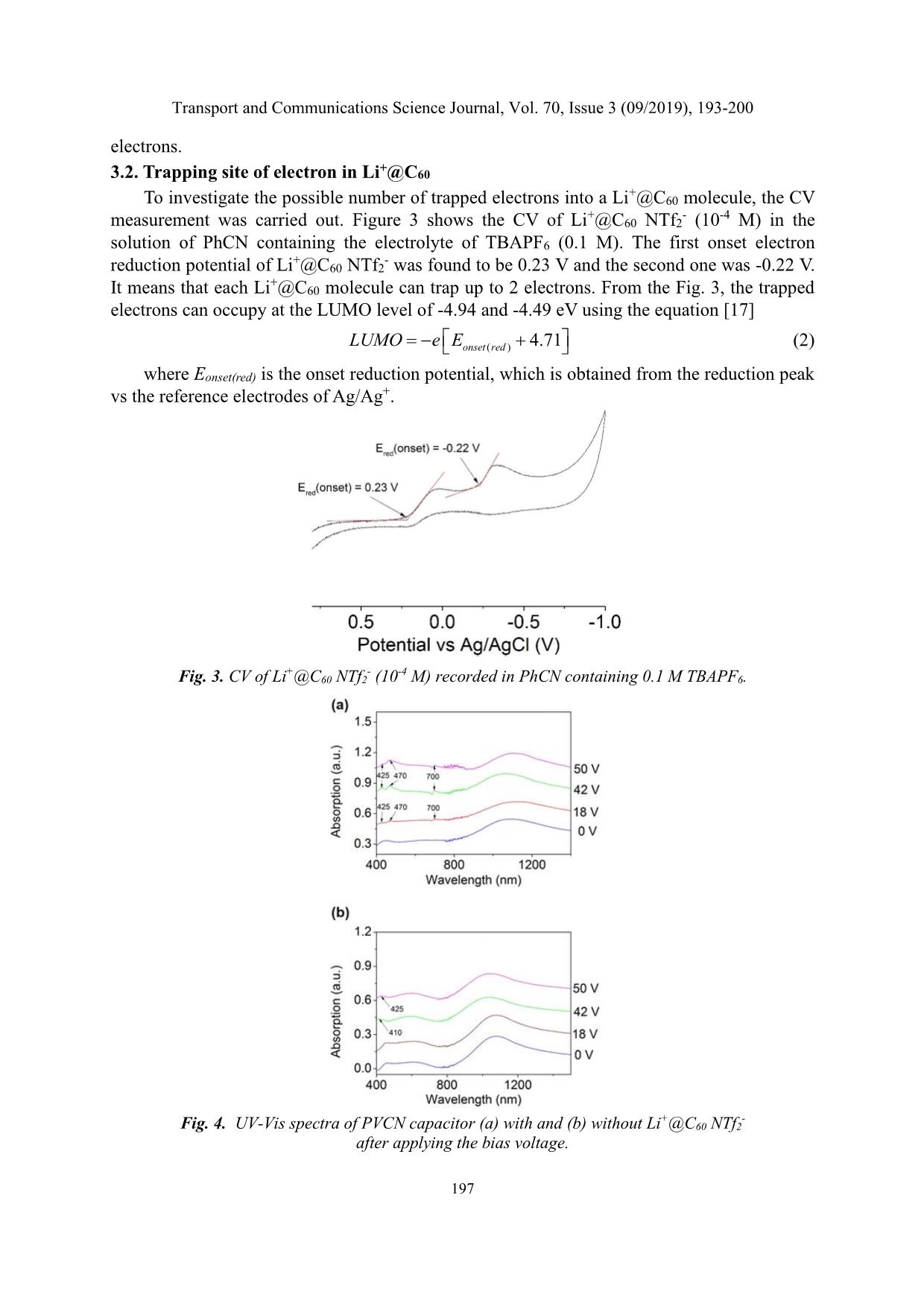
Trang 5
Trang 6
Trang 7
Trang 8
Bạn đang xem tài liệu "Electron trapping mechanism in a multi - level organic fet memory using lithium-ionencapsulated fullerene as the floating gate", để tải tài liệu gốc về máy hãy click vào nút Download ở trên
Tóm tắt nội dung tài liệu: Electron trapping mechanism in a multi - level organic fet memory using lithium-ionencapsulated fullerene as the floating gate
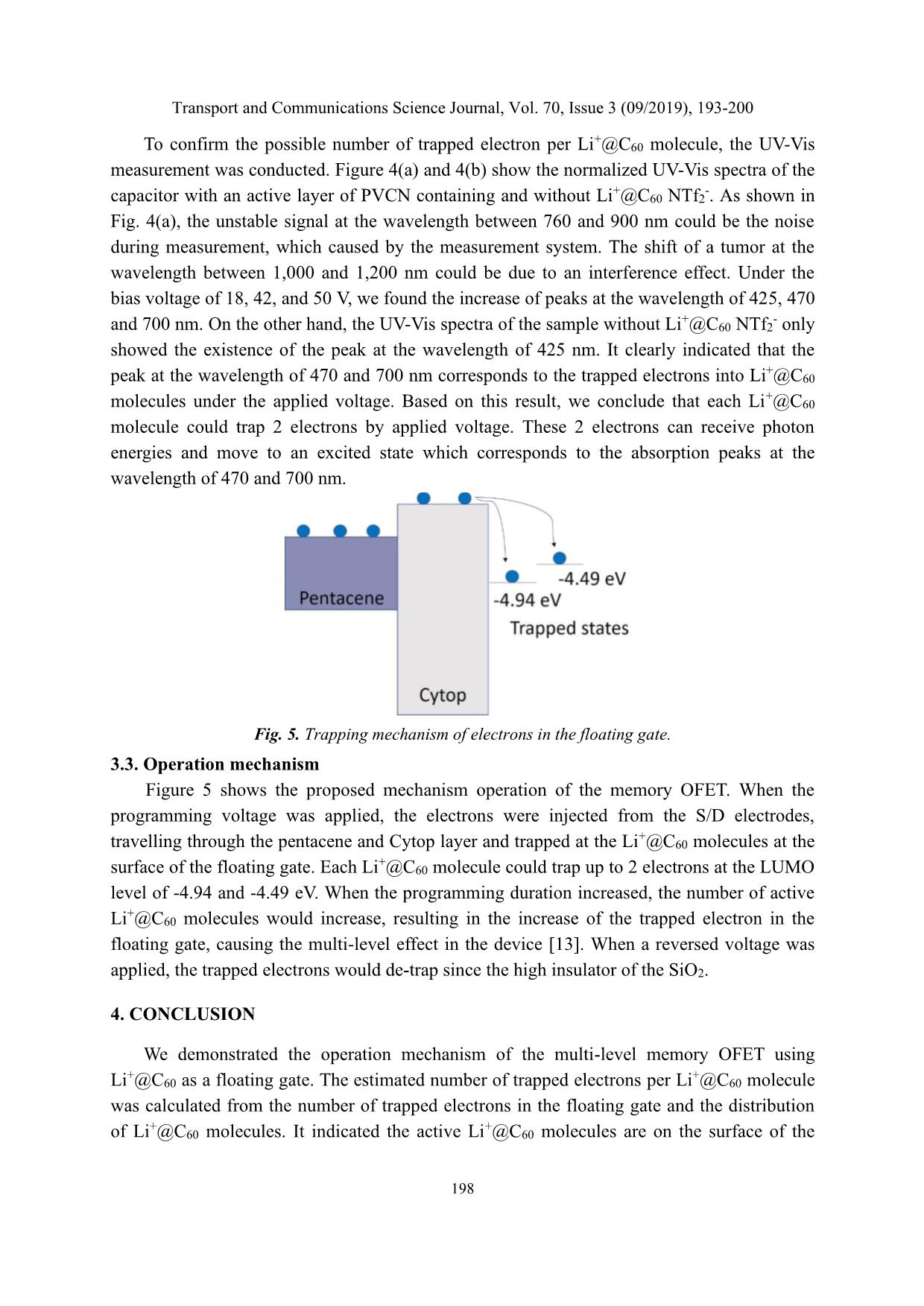
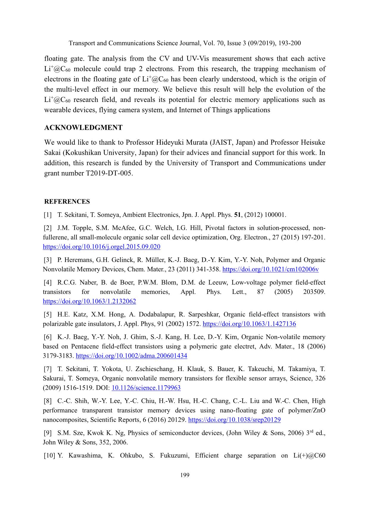
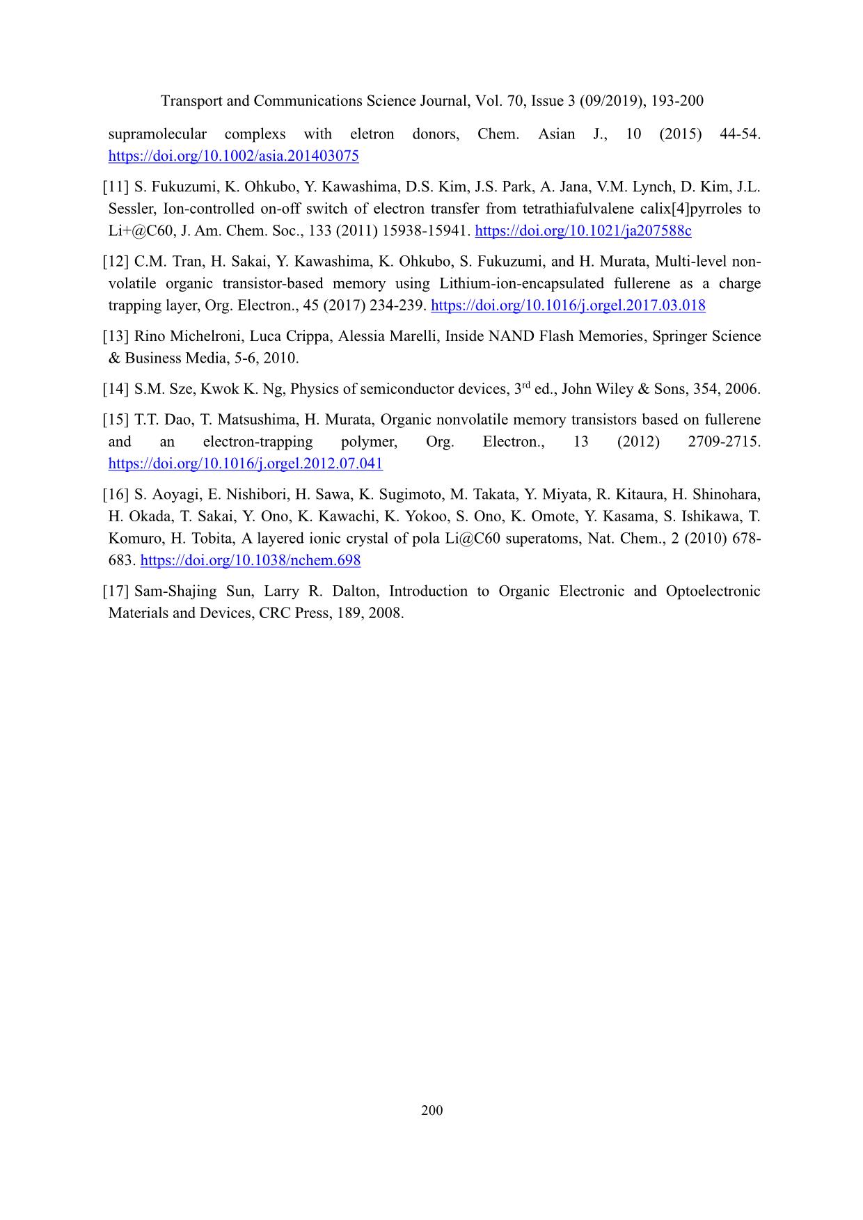
one-electron reduction potential of Li+@C60 is higher than that of pristine fullerene [10,11] indicated that this material is promising to accept electrons. Thus, it is high possible to use Li+@C60 as the floating gate in the memory OFETs. In addition, the multiple reduction/oxidation peaks of Li+@C60 suggests that the number of trapped electrons may be controlled by an applied voltage, which is the key point to fabricate a multi-level memory. The fabrication of the multi-level memory OFETs was presented in our report. [12] These memory devices exhibited multi-level memory characteristics with the ΔVth of 10, 16, 32 V after programming by an applied voltage of 150 V for 0.5, 5, and 50 seconds. The memory effect was concluded to be the trapped electron in the Li+@C60 layer. In this article, we analyze the electron trapping mechanism of the Li+@C60. By estimation the number of trapped electron per each Li+@C60 molecule, we conclude that only Li +@C60 molecules at the surface of the Li+@C60 domains are active, in which electrons are trapped. The cyclic voltammetry (CV) of the Li+@C60 salt was conducted to calculate the trapping site, where electrons are trapped at energy potential of -4.94 and -4.49 eV, respectively. In addition, the ultraviolet-visible spectroscopy (UV-Vis) spectra of Li+@C60 thin film showed 2 absorption peaks at wavelength of 470 and 700 nm, which was an evidence of the trapped electrons in the Li+@C60 molecules under an applied voltage. Transport and Communications Science Journal, Vol. 70, Issue 3 (09/2019), 193-200 195 2. EXPERIMENTAL Figure 1 shows the structure of the memory OFET in this study. The fabrication process of the memory OFET could be found elsewhere in our previous report. [12] To estimate the number of trapped electron in Li+@C60 molecule, the density of trapped electron in the Li+@C60 layer (ΔN) was calculated based on the shift of the Vth. On the other hand, the density of Li+@C60 molecules in floating gate (NLi) was roughly estimated based on the density of Li+@C60 and its distribution in this layer. To clarify the trapping site of electrons in the Li+@C60 molecules, a cyclic voltammetry (CV, Autolab PGSTAT302N by Metrohm) was carried out with a solution of Li+@C60 bis(trifluoromethylsulfonyl)imide (Li+@C60 NTf2 -) in benzonitrile (PhCN) with a concentration of 10-4 M consists of an electrolyte of tetrabutylammonium hexafluorophostate (TBAF6) (0.1 M). The CV measurement was conducted using the working electrode of platinum (Pt), the reference electrode of Ag/Ag+ and the scan rate of 100 mV·s-1. Fig. 1. Schematic structure of the memory OFET. To confirm the electron trapping ability of Li+@C60, a capacitor was prepared for an absorption spectroscopy measurement (Jasco V-570 UV-Vis-NIR Spectrophotometer). On the glass substrate with indium tin oxide (ITO), an active layer of the capacitor was deposited by spin-coating at a speech of 2,500 rpm for 30 second using a solution of a mixture of Li+@C60 NTf2 - and poly vinyl cinnamate (PVCN) (1:8) in mono chlorobenzene with a concentration of 45 mg/ml. Subsequently, the substrate was subjected into ultraviolet exposure for 20 min for photo-crosslinking, followed by dried at 140ºC for 1 h. Finally, an aluminum (Al) electrode was fabricated by thermal deposition. The thickness of the Al electrode was 100 nm. Another capacitor with an active layer of PVCN was prepared under the same fabrication process for comparison. The fabrication and the measurement processes were carried out completely in the cleaning room at Japan Advanced Institute of Science and Technology (JAIST). 3. RESULT AND DISCUSSION 3.1. Electron trapping at Li+@C60 molecule under applied voltage The memory characteristics of the memory OFET which was shown in Fig.1 were presented in our previous report [12]. Under a programming voltage of 150 V for 0.5, 5, and 50 seconds, the transfer curve shift to the positive gate voltage (VG) region, causing the memory window (ΔVth) of 10, 16, and 32 V, respectively. For erasing the data, a reversed Transport and Communications Science Journal, Vol. 70, Issue 3 (09/2019), 193-200 196 voltage of -150 V was used for 0.17, 1.7, and 17 seconds. The memory OFET behaved as a multi-level memory, which was reported in literature [13]. The origin of the memory effect was supposed to be the trapped electron in the Li+@C60 layer. The ΔN was calculated using the equation [14]. th V N d e = (1) where ε, d are the permittivity (1.86 × 10⁻¹³ F·cm-1) [15] and the thickness of the insulator Cytop, e is the elementary charge and ΔVth is the shift of the Vth. Follow our previous report, the ΔN was increased with the duration of programming voltage [12]. The density of the floating gate (NLi) can be estimated from the its distribution on the SiO2 surface and the molecular density of Li +@C60 salt if this layer was stable after the insulator fabrication. Figure 2(a) and 2(b) show the morphology of Li+@C60 on the SiO2 surface before and after spin-coating the insulator of Cytop (AFM, Hitachi SPA 400). As shown in the Fig. 2a, the Li+@C60 layer was formed as domains on the SiO2 surface. These domains are still observed after the insulator fabrication (Fig. 2(b)). It indicated that the Li+@C60 are stable and would act as the floating gate in the memory device. Since the Li+@C60 domains distributed as islands on the SiO2 surface, we assumed that the average roughness (Sa) of this surface is refer to the thickness of the floating gate. The Sa was estimated to be 8.00 nm. S. Aoyagi et al. reported a cubic of Li+@C60 hexa-chloroantimonate (Li+@C60 SbCl6 -) contained 4 molecules had a volume of 3,554.6 Å3. [16]. We assumed that the crystal structure of Li+@C60 NTf2 - was similar with those of Li+@C60 SbCl6 -. Thus, the molecular density of Li+@C60 NTf2 - was estimated to be 1.88 g·mol-1. Based on these results, the NLi was roughly estimated to be 9.00 × 10 14 cm-2. Fig. 2. Morphology with a cross section profile of Li+@C60 layer on the SiO2 surface (a) before and (b) after spin-coating a layer of Cytop. Under the programming voltage of 150 V for 0.5, 5 and 50 s, count per area unit, ΔN electrons would be injected into NLi Li +@C60 molecules of the floating gate. If all Li +@C60 molecules had trapped electrons, the average number of trapped electron per Li+@C60 molecule would have been 2.40 × 10⁻², 3.84× 10⁻², and 7.68 × 10 -2 electrons, respectively. It indicated that electrons would not be trapped by all Li+@C60 molecules. We proposed that only the Li+@C60 molecules at the surface of the floating gate were active and trapped the Transport and Communications Science Journal, Vol. 70, Issue 3 (09/2019), 193-200 197 electrons. 3.2. Trapping site of electron in Li+@C60 To investigate the possible number of trapped electrons into a Li+@C60 molecule, the CV measurement was carried out. Figure 3 shows the CV of Li+@C60 NTf2 - (10-4 M) in the solution of PhCN containing the electrolyte of TBAPF6 (0.1 M). The first onset electron reduction potential of Li+@C60 NTf2 - was found to be 0.23 V and the second one was -0.22 V. It means that each Li+@C60 molecule can trap up to 2 electrons. From the Fig. 3, the trapped electrons can occupy at the LUMO level of -4.94 and -4.49 eV using the equation [17] ( ) 4.71onset redLUMO e E = − + (2) where Eonset(red) is the onset reduction potential, which is obtained from the reduction peak vs the reference electrodes of Ag/Ag+. Fig. 3. CV of Li+@C60 NTf2 - (10-4 M) recorded in PhCN containing 0.1 M TBAPF6. Fig. 4. UV-Vis spectra of PVCN capacitor (a) with and (b) without Li+@C60 NTf2 - after applying the bias voltage. Transport and Communications Science Journal, Vol. 70, Issue 3 (09/2019), 193-200 198 To confirm the possible number of trapped electron per Li+@C60 molecule, the UV-Vis measurement was conducted. Figure 4(a) and 4(b) show the normalized UV-Vis spectra of the capacitor with an active layer of PVCN containing and without Li+@C60 NTf2 -. As shown in Fig. 4(a), the unstable signal at the wavelength between 760 and 900 nm could be the noise during measurement, which caused by the measurement system. The shift of a tumor at the wavelength between 1,000 and 1,200 nm could be due to an interference effect. Under the bias voltage of 18, 42, and 50 V, we found the increase of peaks at the wavelength of 425, 470 and 700 nm. On the other hand, the UV-Vis spectra of the sample without Li+@C60 NTf2 - only showed the existence of the peak at the wavelength of 425 nm. It clearly indicated that the peak at the wavelength of 470 and 700 nm corresponds to the trapped electrons into Li+@C60 molecules under the applied voltage. Based on this result, we conclude that each Li+@C60 molecule could trap 2 electrons by applied voltage. These 2 electrons can receive photon energies and move to an excited state which corresponds to the absorption peaks at the wavelength of 470 and 700 nm. Fig. 5. Trapping mechanism of electrons in the floating gate. 3.3. Operation mechanism Figure 5 shows the proposed mechanism operation of the memory OFET. When the programming voltage was applied, the electrons were injected from the S/D electrodes, travelling through the pentacene and Cytop layer and trapped at the Li+@C60 molecules at the surface of the floating gate. Each Li+@C60 molecule could trap up to 2 electrons at the LUMO level of -4.94 and -4.49 eV. When the programming duration increased, the number of active Li+@C60 molecules would increase, resulting in the increase of the trapped electron in the floating gate, causing the multi-level effect in the device [13]. When a reversed voltage was applied, the trapped electrons would de-trap since the high insulator of the SiO2. 4. CONCLUSION We demonstrated the operation mechanism of the multi-level memory OFET using Li+@C60 as a floating gate. The estimated number of trapped electrons per Li +@C60 molecule was calculated from the number of trapped electrons in the floating gate and the distribution of Li+@C60 molecules. It indicated the active Li +@C60 molecules are on the surface of the Transport and Communications Science Journal, Vol. 70, Issue 3 (09/2019), 193-200 199 floating gate. The analysis from the CV and UV-Vis measurement shows that each active Li+@C60 molecule could trap 2 electrons. From this research, the trapping mechanism of electrons in the floating gate of Li+@C60 has been clearly understood, which is the origin of the multi-level effect in our memory. We believe this result will help the evolution of the Li+@C60 research field, and reveals its potential for electric memory applications such as wearable devices, flying camera system, and Internet of Things applications ACKNOWLEDGMENT We would like to thank to Professor Hideyuki Murata (JAIST, Japan) and Professor Heisuke Sakai (Kokushikan University, Japan) for their advices and financial support for this work. In addition, this research is funded by the University of Transport and Communications under grant number T2019-DT-005. REFERENCES [1] T. Sekitani, T. Someya, Ambient Electronics, Jpn. J. Appl. Phys. 51, (2012) 100001. [2] J.M. Topple, S.M. McAfee, G.C. Welch, I.G. Hill, Pivotal factors in solution-processed, non- fullerene, all small-molecule organic solar cell device optimization, Org. Electron., 27 (2015) 197-201. https://doi.org/10.1016/j.orgel.2015.09.020 [3] P. Heremans, G.H. Gelinck, R. Müller, K.-J. Baeg, D.-Y. Kim, Y.-Y. Noh, Polymer and Organic Nonvolatile Memory Devices, Chem. Mater., 23 (2011) 341-358. https://doi.org/10.1021/cm102006v [4] R.C.G. Naber, B. de Boer, P.W.M. Blom, D.M. de Leeuw, Low-voltage polymer field-effect transistors for nonvolatile memories, Appl. Phys. Lett., 87 (2005) 203509. https://doi.org/10.1063/1.2132062 [5] H.E. Katz, X.M. Hong, A. Dodabalapur, R. Sarpeshkar, Organic field-effect transistors with polarizable gate insulators, J. Appl. Phys, 91 (2002) 1572. https://doi.org/10.1063/1.1427136 [6] K.-J. Baeg, Y.-Y. Noh, J. Ghim, S.-J. Kang, H. Lee, D.-Y. Kim, Organic Non-volatile memory based on Pentacene field-effect transistors using a polymeric gate electret, Adv. Mater., 18 (2006) 3179-3183. https://doi.org/10.1002/adma.200601434 [7] T. Sekitani, T. Yokota, U. Zschieschang, H. Klauk, S. Bauer, K. Takeuchi, M. Takamiya, T. Sakurai, T. Someya, Organic nonvolatile memory transistors for flexible sensor arrays, Science, 326 (2009) 1516-1519. DOI: 10.1126/science.1179963 [8] C.-C. Shih, W.-Y. Lee, Y.-C. Chiu, H.-W. Hsu, H.-C. Chang, C.-L. Liu and W.-C. Chen, High performance transparent transistor memory devices using nano-floating gate of polymer/ZnO nanocomposites, Scientific Reports, 6 (2016) 20129. https://doi.org/10.1038/srep20129 [9] S.M. Sze, Kwok K. Ng, Physics of semiconductor devices, (John Wiley & Sons, 2006) 3rd ed., John Wiley & Sons, 352, 2006. [10] Y. Kawashima, K. Ohkubo, S. Fukuzumi, Efficient charge separation on Li(+)@C60 Transport and Communications Science Journal, Vol. 70, Issue 3 (09/2019), 193-200 200 supramolecular complexs with eletron donors, Chem. Asian J., 10 (2015) 44-54. https://doi.org/10.1002/asia.201403075 [11] S. Fukuzumi, K. Ohkubo, Y. Kawashima, D.S. Kim, J.S. Park, A. Jana, V.M. Lynch, D. Kim, J.L. Sessler, Ion-controlled on-off switch of electron transfer from tetrathiafulvalene calix[4]pyrroles to Li+@C60, J. Am. Chem. Soc., 133 (2011) 15938-15941. https://doi.org/10.1021/ja207588c [12] C.M. Tran, H. Sakai, Y. Kawashima, K. Ohkubo, S. Fukuzumi, and H. Murata, Multi-level non- volatile organic transistor-based memory using Lithium-ion-encapsulated fullerene as a charge trapping layer, Org. Electron., 45 (2017) 234-239. https://doi.org/10.1016/j.orgel.2017.03.018 [13] Rino Michelroni, Luca Crippa, Alessia Marelli, Inside NAND Flash Memories, Springer Science & Business Media, 5-6, 2010. [14] S.M. Sze, Kwok K. Ng, Physics of semiconductor devices, 3rd ed., John Wiley & Sons, 354, 2006. [15] T.T. Dao, T. Matsushima, H. Murata, Organic nonvolatile memory transistors based on fullerene and an electron-trapping polymer, Org. Electron., 13 (2012) 2709-2715. https://doi.org/10.1016/j.orgel.2012.07.041 [16] S. Aoyagi, E. Nishibori, H. Sawa, K. Sugimoto, M. Takata, Y. Miyata, R. Kitaura, H. Shinohara, H. Okada, T. Sakai, Y. Ono, K. Kawachi, K. Yokoo, S. Ono, K. Omote, Y. Kasama, S. Ishikawa, T. Komuro, H. Tobita, A layered ionic crystal of pola Li@C60 superatoms, Nat. Chem., 2 (2010) 678- 683. https://doi.org/10.1038/nchem.698 [17] Sam-Shajing Sun, Larry R. Dalton, Introduction to Organic Electronic and Optoelectronic Materials and Devices, CRC Press, 189, 2008.
File đính kèm:
 electron_trapping_mechanism_in_a_multi_level_organic_fet_mem.pdf

