Design and simulation of scanning probe micro - cantilever for the scanning probe lithography
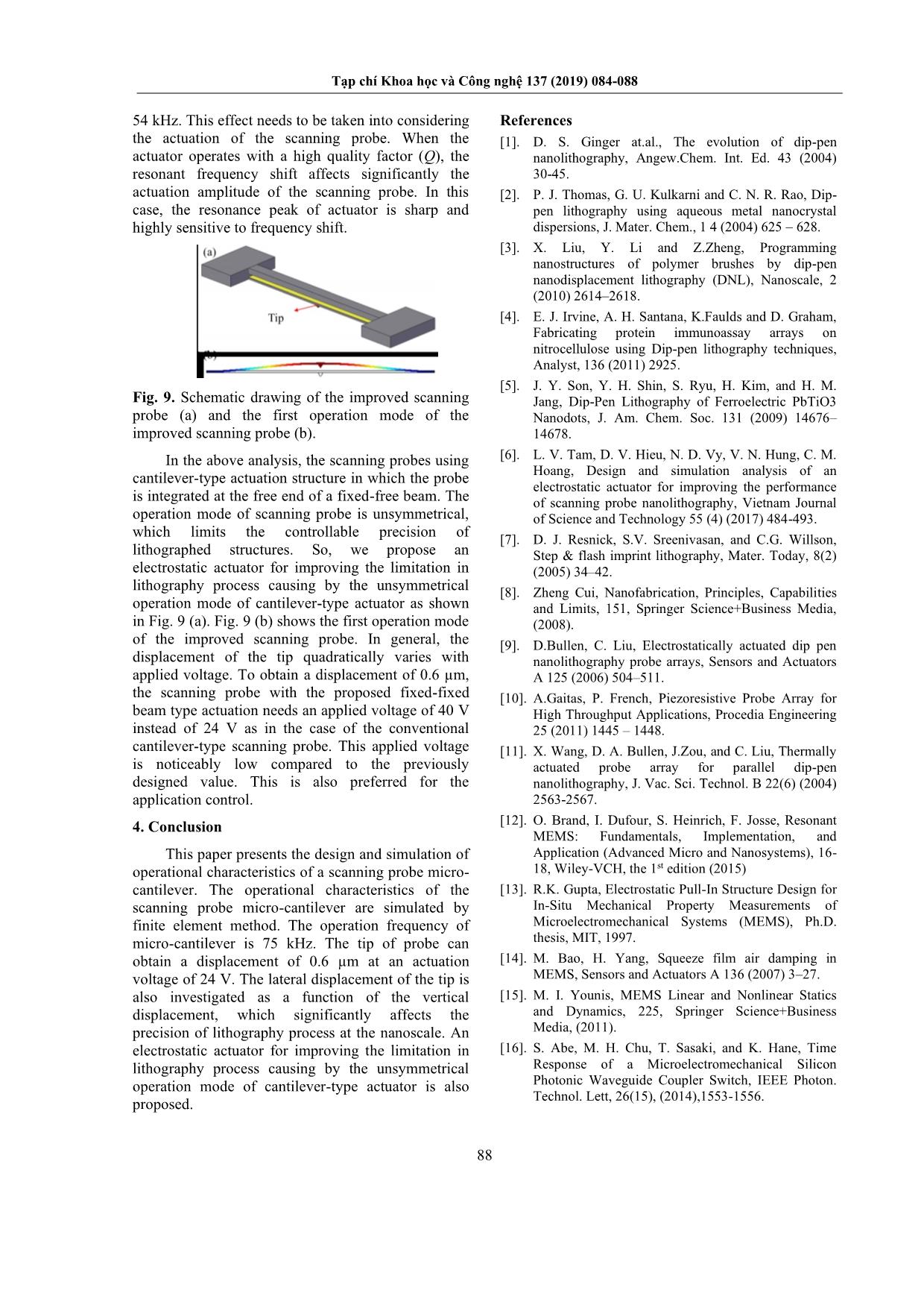
Trong bài báo này, chúng tôi báo cáo về thiết kế và mô phỏng một vi đầu dò quét. Vi đầu dò quét bao gồm
một mũi nhọn silicon, được tích hợp ở đầu tự do của thanh dầm treo silicon. Vi đầu dò quét được điều khiển
tĩnh điện bằng cách sử dụng chấp hành dạng điện dung điện cực song song. Mũi nhọn silicon có dạng hình
chóp tứ giác đều, được tạo ra bằng cách ăn mòn dị hướng silicon đơn tinh thể trong dung dịch kali hydroxit.
Một điện cực được đặt phía trên mặt sau của thanh dầm treo với một khe hở để tạo ra chấp hành kiểu điện
dung. Các đặc trưng hoạt động của vi đầu dò được mô phỏng bằng phương pháp phần tử hữu hạn. Độ dịch
chuyển của đầu dò quét và biến đổi điện dung phụ thuộc vào điện áp tác dụng đã được nghiên cứu. Đặc
trưng hoạt động của đầu dò trong môi trường không khí cũng được khảo sát. Vi đầu dò được thiết kế cho
ứng dụng trong khắc đầu dò quét.
Trang 1
Trang 2
Trang 3
Trang 4
Trang 5
Tóm tắt nội dung tài liệu: Design and simulation of scanning probe micro - cantilever for the scanning probe lithography
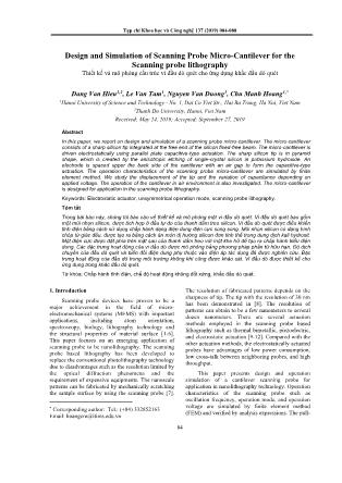
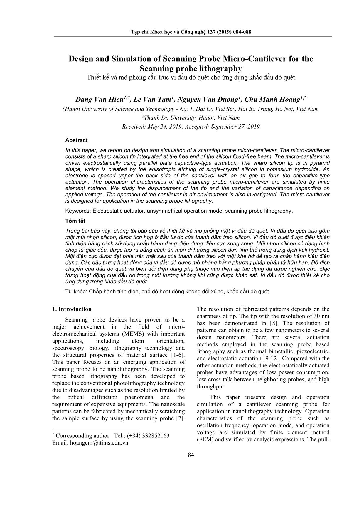
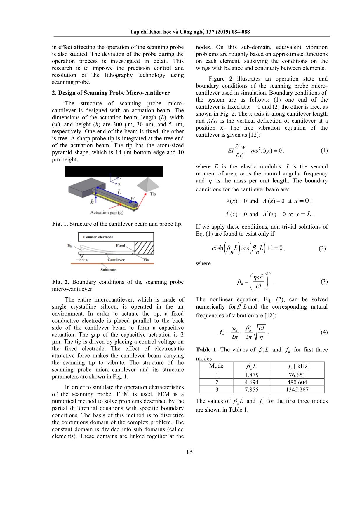
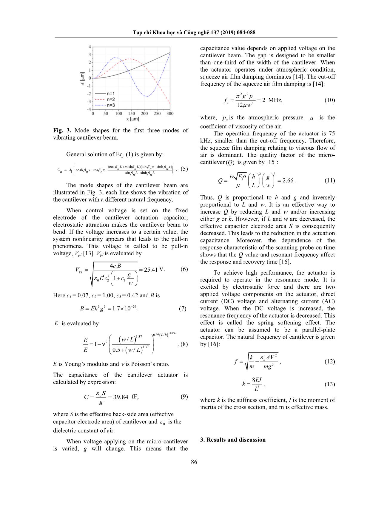
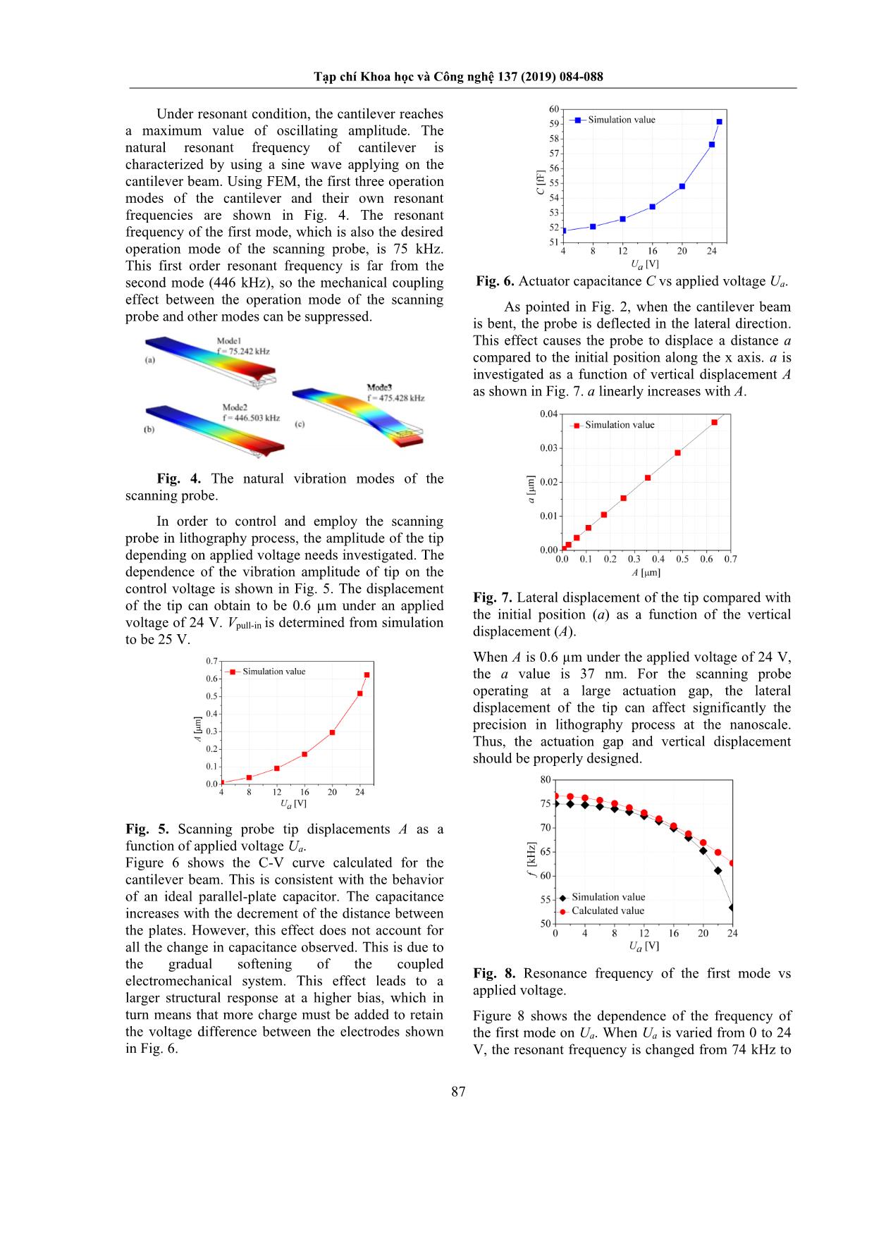
ation voltage are simulated by finite element method (FEM) and verified by analysis expressions. The pull- Tạp chí Khoa học và Công nghệ 137 (2019) 084-088 85 in effect affecting the operation of the scanning probe is also studied. The deviation of the probe during the operation process is investigated in detail. This research is to improve the precision control and resolution of the lithography technology using scanning probe. 2. Design of Scanning Probe Micro-cantilever The structure of scanning probe micro- cantilever is designed with an actuation beam. The dimensions of the actuation beam, length (L), width (w), and height (h) are 300 μm, 30 μm, and 5 μm, respectively. One end of the beam is fixed, the other is free. A sharp probe tip is integrated at the free end of the actuation beam. The tip has the atom-sized pyramid shape, which is 14 μm bottom edge and 10 μm height. Fig. 1. Structure of the cantilever beam and probe tip. Fig. 2. Boundary conditions of the scanning probe micro-cantilever. The entire microcantilever, which is made of single crystalline silicon, is operated in the air environment. In order to actuate the tip, a fixed conductive electrode is placed parallel to the back side of the cantilever beam to form a capacitive actuation. The gap of the capacitive actuation is 2 µm. The tip is driven by placing a control voltage on the fixed electrode. The effect of electrostatic attractive force makes the cantilever beam carrying the scanning tip to vibrate. The structure of the scanning probe micro-cantilever and its structure parameters are shown in Fig. 1. In order to simulate the operation characteristics of the scanning probe, FEM is used. FEM is a numerical method to solve problems described by the partial differential equations with specific boundary conditions. The basis of this method is to discretize the continuous domain of the complex problem. The constant domain is divided into sub domains (called elements). These domains are linked together at the nodes. On this sub-domain, equivalent vibration problems are roughly based on approximate functions on each element, satisfying the conditions on the wings with balance and continuity between elements. Figure 2 illustrates an operation state and boundary conditions of the scanning probe micro- cantilever used in simulation. Boundary conditions of the system are as follows: (1) one end of the cantilever is fixed at x = 0 and (2) the other is free, as shown in Fig. 2. The x axis is along cantilever length and A(x) is the vertical deflection of cantilever at a position x. The free vibration equation of the cantilever is given as [12]: 4 2 4 ( ) 0 w EI A x x − = , (1) where E is the elastic modulus, I is the second moment of area, ω is the natural angular frequency and is the mass per unit length. The boundary conditions for the cantilever beam are: ( ) 0A x = and ' ( ) 0A x = at 0x = ; '' ( ) 0A x = and ''' ( ) 0A x = at x L= . If we apply these conditions, non-trivial solutions of Eq. (1) are found to exist only if ( ) ( )osh os 1 0c L c Ln n + = , (2) where 1/4 2 n EI = . (3) The nonlinear equation, Eq. (2), can be solved numerically for nL and the corresponding natural frequencies of vibration are [12]: 2 2 2 n n n EI f = = . (4) Table 1. The values of nL and nf for first three modes Mode nL nf [ kHz] 1 1.875 76.651 2 4.694 480.604 3 7.855 1345.267 The values of nL and nf for the first three modes are shown in Table 1. Tạp chí Khoa học và Công nghệ 137 (2019) 084-088 86 Fig. 3. Mode shapes for the first three modes of vibrating cantilever beam. General solution of Eq. (1) is given by: (cos osh )(sin sinh ) ˆ cosh os1 sin sinh L c L x x n n n nw A x c xn n n L L n n + − = − + + . (5) The mode shapes of the cantilever beam are illustrated in Fig. 3, each line shows the vibration of the cantilever with a different natural frequency. When control voltage is set on the fixed electrode of the cantilever actuation capacitor, electrostatic attraction makes the cantilever beam to bend. If the voltage increases to a certain value, the system nonlinearity appears that leads to the pull-in phenomena. This voltage is called to be pull-in voltage, Vpi [13]. Vpi is evaluated by 1 4 2 0 2 3 4 25.41 1 PI c B V g L c c w = = + V. (6) Here c1 = 0.07, c2 = 1.00, c3 = 0.42 and B is 3 3 261.7 10B Eh g −= = . (7) E is evaluated by ( ) ( ) ( ) 0.056 0.98 / 1.37 2 1.37 / 1 0.5 / L h w LE E w L − = − + . (8) E is Young’s modulus and is Poisson’s ratio. The capacitance of the cantilever actuator is calculated by expression: 39.84o S C g = = fF, (9) where S is the effective back-side area (effective capacitor electrode area) of cantilever and 0 is the dielectric constant of air. When voltage applying on the micro-cantilever is varied, g will change. This means that the capacitance value depends on applied voltage on the cantilever beam. The gap is designed to be smaller than one-third of the width of the cantilever. When the actuator operates under atmospheric condition, squeeze air film damping dominates [14]. The cut-off frequency of the squeeze air film damping is [14]: 2 2 2 2 12 a c g p f w = = MHz, (10) where, ap is the atmospheric pressure. is the coefficient of viscosity of the air. The operation frequency of the actuator is 75 kHz, smaller than the cut-off frequency. Therefore, the squeeze film damping relating to viscous flow of air is dominant. The quality factor of the micro- cantilever ( )Q is given by [15]: 2 3 2.66 w E h g Q L w = = . (11) Thus, Q is proportional to h and g and inversely proportional to L and w. It is an effective way to increase Q by reducing L and w and/or increasing either g or h. However, if L and w are decreased, the effective capacitor electrode area S is consequently decreased. This leads to the reduction in the actuation capacitance. Moreover, the dependence of the response characteristic of the scanning probe on time shows that the Q value and resonant frequency affect the response and recovery time [16]. To achieve high performance, the actuator is required to operate in the resonance mode. It is excited by electrostatic force and there are two applied voltage components on the actuator, direct current (DC) voltage and alternating current (AC) voltage. When the DC voltage is increased, the resonance frequency of the actuator is decreased. This effect is called the spring softening effect. The actuator can be assumed to be a parallel-plate capacitor. The natural frequency of cantilever is given by [16]: 2 3 oAVkf m mg = − , (12) 3 8EI k L = , (13) where k is the stiffness coefficient, I is the moment of inertia of the cross section, and m is effective mass. 3. Results and discussion Tạp chí Khoa học và Công nghệ 137 (2019) 084-088 87 Under resonant condition, the cantilever reaches a maximum value of oscillating amplitude. The natural resonant frequency of cantilever is characterized by using a sine wave applying on the cantilever beam. Using FEM, the first three operation modes of the cantilever and their own resonant frequencies are shown in Fig. 4. The resonant frequency of the first mode, which is also the desired operation mode of the scanning probe, is 75 kHz. This first order resonant frequency is far from the second mode (446 kHz), so the mechanical coupling effect between the operation mode of the scanning probe and other modes can be suppressed. Fig. 4. The natural vibration modes of the scanning probe. In order to control and employ the scanning probe in lithography process, the amplitude of the tip depending on applied voltage needs investigated. The dependence of the vibration amplitude of tip on the control voltage is shown in Fig. 5. The displacement of the tip can obtain to be 0.6 µm under an applied voltage of 24 V. Vpull-in is determined from simulation to be 25 V. Fig. 5. Scanning probe tip displacements A as a function of applied voltage Ua. Figure 6 shows the C-V curve calculated for the cantilever beam. This is consistent with the behavior of an ideal parallel-plate capacitor. The capacitance increases with the decrement of the distance between the plates. However, this effect does not account for all the change in capacitance observed. This is due to the gradual softening of the coupled electromechanical system. This effect leads to a larger structural response at a higher bias, which in turn means that more charge must be added to retain the voltage difference between the electrodes shown in Fig. 6. Fig. 6. Actuator capacitance C vs applied voltage Ua. As pointed in Fig. 2, when the cantilever beam is bent, the probe is deflected in the lateral direction. This effect causes the probe to displace a distance a compared to the initial position along the x axis. a is investigated as a function of vertical displacement A as shown in Fig. 7. a linearly increases with A. Fig. 7. Lateral displacement of the tip compared with the initial position (a) as a function of the vertical displacement (A). When A is 0.6 µm under the applied voltage of 24 V, the a value is 37 nm. For the scanning probe operating at a large actuation gap, the lateral displacement of the tip can affect significantly the precision in lithography process at the nanoscale. Thus, the actuation gap and vertical displacement should be properly designed. Fig. 8. Resonance frequency of the first mode vs applied voltage. Figure 8 shows the dependence of the frequency of the first mode on Ua. When Ua is varied from 0 to 24 V, the resonant frequency is changed from 74 kHz to Tạp chí Khoa học và Công nghệ 137 (2019) 084-088 88 54 kHz. This effect needs to be taken into considering the actuation of the scanning probe. When the actuator operates with a high quality factor (Q), the resonant frequency shift affects significantly the actuation amplitude of the scanning probe. In this case, the resonance peak of actuator is sharp and highly sensitive to frequency shift. Fig. 9. Schematic drawing of the improved scanning probe (a) and the first operation mode of the improved scanning probe (b). In the above analysis, the scanning probes using cantilever-type actuation structure in which the probe is integrated at the free end of a fixed-free beam. The operation mode of scanning probe is unsymmetrical, which limits the controllable precision of lithographed structures. So, we propose an electrostatic actuator for improving the limitation in lithography process causing by the unsymmetrical operation mode of cantilever-type actuator as shown in Fig. 9 (a). Fig. 9 (b) shows the first operation mode of the improved scanning probe. In general, the displacement of the tip quadratically varies with applied voltage. To obtain a displacement of 0.6 µm, the scanning probe with the proposed fixed-fixed beam type actuation needs an applied voltage of 40 V instead of 24 V as in the case of the conventional cantilever-type scanning probe. This applied voltage is noticeably low compared to the previously designed value. This is also preferred for the application control. 4. Conclusion This paper presents the design and simulation of operational characteristics of a scanning probe micro- cantilever. The operational characteristics of the scanning probe micro-cantilever are simulated by finite element method. The operation frequency of micro-cantilever is 75 kHz. The tip of probe can obtain a displacement of 0.6 µm at an actuation voltage of 24 V. The lateral displacement of the tip is also investigated as a function of the vertical displacement, which significantly affects the precision of lithography process at the nanoscale. An electrostatic actuator for improving the limitation in lithography process causing by the unsymmetrical operation mode of cantilever-type actuator is also proposed. References [1]. D. S. Ginger at.al., The evolution of dip-pen nanolithography, Angew.Chem. Int. Ed. 43 (2004) 30-45. [2]. P. J. Thomas, G. U. Kulkarni and C. N. R. Rao, Dip- pen lithography using aqueous metal nanocrystal dispersions, J. Mater. Chem., 1 4 (2004) 625 – 628. [3]. X. Liu, Y. Li and Z.Zheng, Programming nanostructures of polymer brushes by dip-pen nanodisplacement lithography (DNL), Nanoscale, 2 (2010) 2614–2618. [4]. E. J. Irvine, A. H. Santana, K.Faulds and D. Graham, Fabricating protein immunoassay arrays on nitrocellulose using Dip-pen lithography techniques, Analyst, 136 (2011) 2925. [5]. J. Y. Son, Y. H. Shin, S. Ryu, H. Kim, and H. M. Jang, Dip-Pen Lithography of Ferroelectric PbTiO3 Nanodots, J. Am. Chem. Soc. 131 (2009) 14676– 14678. [6]. L. V. Tam, D. V. Hieu, N. D. Vy, V. N. Hung, C. M. Hoang, Design and simulation analysis of an electrostatic actuator for improving the performance of scanning probe nanolithography, Vietnam Journal of Science and Technology 55 (4) (2017) 484-493. [7]. D. J. Resnick, S.V. Sreenivasan, and C.G. Willson, Step & flash imprint lithography, Mater. Today, 8(2) (2005) 34–42. [8]. Zheng Cui, Nanofabrication, Principles, Capabilities and Limits, 151, Springer Science+Business Media, (2008). [9]. D.Bullen, C. Liu, Electrostatically actuated dip pen nanolithography probe arrays, Sensors and Actuators A 125 (2006) 504–511. [10]. A.Gaitas, P. French, Piezoresistive Probe Array for High Throughput Applications, Procedia Engineering 25 (2011) 1445 – 1448. [11]. X. Wang, D. A. Bullen, J.Zou, and C. Liu, Thermally actuated probe array for parallel dip-pen nanolithography, J. Vac. Sci. Technol. B 22(6) (2004) 2563-2567. [12]. O. Brand, I. Dufour, S. Heinrich, F. Josse, Resonant MEMS: Fundamentals, Implementation, and Application (Advanced Micro and Nanosystems), 16- 18, Wiley-VCH, the 1st edition (2015) [13]. R.K. Gupta, Electrostatic Pull-In Structure Design for In-Situ Mechanical Property Measurements of Microelectromechanical Systems (MEMS), Ph.D. thesis, MIT, 1997. [14]. M. Bao, H. Yang, Squeeze film air damping in MEMS, Sensors and Actuators A 136 (2007) 3–27. [15]. M. I. Younis, MEMS Linear and Nonlinear Statics and Dynamics, 225, Springer Science+Business Media, (2011). [16]. S. Abe, M. H. Chu, T. Sasaki, and K. Hane, Time Response of a Microelectromechanical Silicon Photonic Waveguide Coupler Switch, IEEE Photon. Technol. Lett, 26(15), (2014),1553-1556.
File đính kèm:
 design_and_simulation_of_scanning_probe_micro_cantilever_for.pdf

