Design a 2x2 compact mode switching using multimode interference based on silicon material
We propose a new design of a 2x2 optical chip for switching optical modes based
on silicon material. Input lights at fundamental mode of transverse electric (TE) polarization
can be selected at the output by appropriately controlling a 180-degree butterfly-shaped phase
shifter. The proposed device consists of two multimode interference waveguides MMI and a
phase shifter packed in a compact size of 4.2μm x 0.22μm x 110.4μm. We use 3D-BPM
numerical simulation method to evaluate optical conversion efficiency of device. The result
shows that insertion loss is always less than 1.5dB and crosstalk is always below -30dB in a
wavelength range from 1.5𝜇𝑚 to 1.6𝜇𝑚. Moreover, we continue to evaluate the proposed
device on the system with signal’s bitrate of 35Gbps, the bit error rate is always less than 10-
10 in the whole bandwidth of 100nm.
Trang 1
Trang 2
Trang 3
Trang 4
Trang 5
Trang 6
Trang 7
Trang 8
Trang 9
Trang 10
Tải về để xem bản đầy đủ
Tóm tắt nội dung tài liệu: Design a 2x2 compact mode switching using multimode interference based on silicon material
division multiplexing switching device on optical
chip that has been demonstrated experimentally using a Y junction structure and a MMI coupler
[17]. The switching between the ports is achieved by a lateral PN junction. The device can perform
switches for 2 modes TE0 and TE1, simulated insertion loss is less than 0.3dB for both TE0 and TE1
inputs over the wavelength range from 1530nm to 1570nm but a disadvantage of this device is
quite large in size, approximately 400μm in length. Next, another research used 2 MMI couplers
and a thermo-optic phase shifter to design a switching device [18], but the device’s insertion loss
is quite high up to 1dB at the central wavelength. However, the general characteristics of those
devices has not evaluated performance on the system.
In this paper, we study to combine the advantages of these two MMI structures to create a
2x2 mode switching device using silicon on insulator with switching the modes TE0 between two
inputs and two outputs. The high optical conversion efficiency over 97% and compact size of
4.2𝜇𝑚 x 0.22𝜇𝑚 x 110.4𝜇𝑚 are advantages of the proposed device. In addition, we evaluate the
fabrication tolerance of the device, the results demonstrate that the device can work well with a
large manufacturing errors. Moreover, we also evaluate the effectiveness of devices on complex
communication systems, the simulation results show that the device can operate effectively with
performance more than 70% in a wide bandwidth up to 100nm. Furthermore, the proposed device
can work with an extremely high bit rate of up to 35Gbps while bit error rate is always remained
smaller than 10-10.
2 Device structure and design principle.
2.1 MMI theory
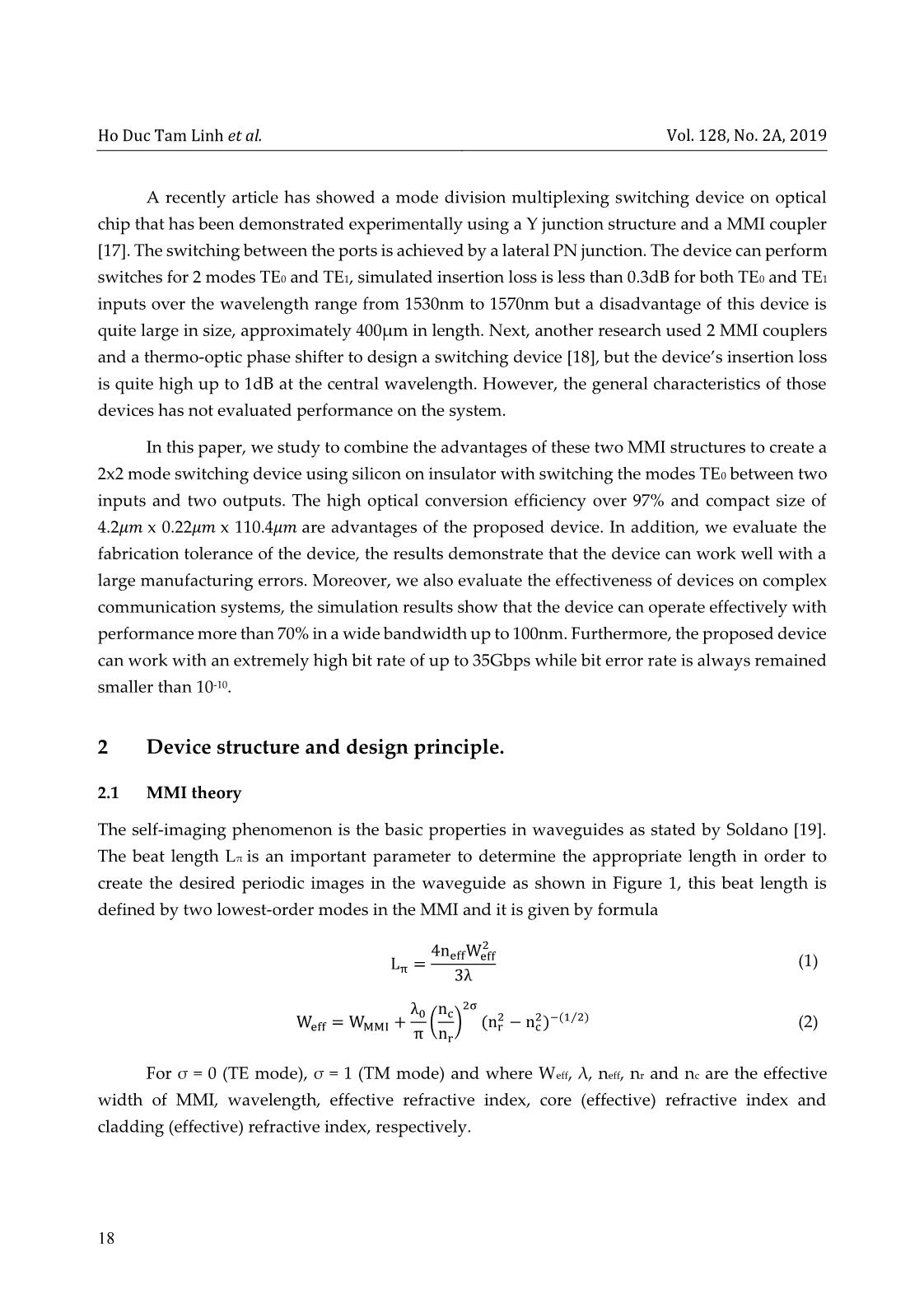
The self-imaging phenomenon is the basic properties in waveguides as stated by Soldano [19].
The beat length Lπ is an important parameter to determine the appropriate length in order to
create the desired periodic images in the waveguide as shown in Figure 1, this beat length is
defined by two lowest-order modes in the MMI and it is given by formula
Lπ =
4neffWeff
2
3λ
 (1)
Weff = WMMI +
λ0
π
(
nc
nr
)
2σ
(nr
2 − nc
2)−(1 2)⁄ (2)
For σ = 0 (TE mode), σ = 1 (TM mode) and where Weff, λ, neff, nr and nc are the effective
width of MMI, wavelength, effective refractive index, core (effective) refractive index and
cladding (effective) refractive index, respectively.
jos.hueuni.edu.vn Vol. 128, No. 2A, 2018
19
Fig. 1. The self-imaging theory in 2×2 MMI coupler
The self-imaging in waveguide is created by one of two interference mechanisms: general
interference and restricted interference mechanisms.
For general interference mechanism is shown by formula
LMMI =
p
N
(3Lπ) (3)
And restricted interference mechanism
LMMI =
p
N
(Lπ) (4)
Where N is the number of input and output ports of the MMI, p denotes the periodic
properties of image along the MMI. We usually choose p = 1 to shorten the size of the device as
much as possible. Comparing between two interference mechanisms above, notice that the length
of devices using the restricted interference mechanism is three times shorter than that using the
general interference mechanism.
2.2 Phase shifter
The phase shifter plays an important role in this article with the aim of controlling the
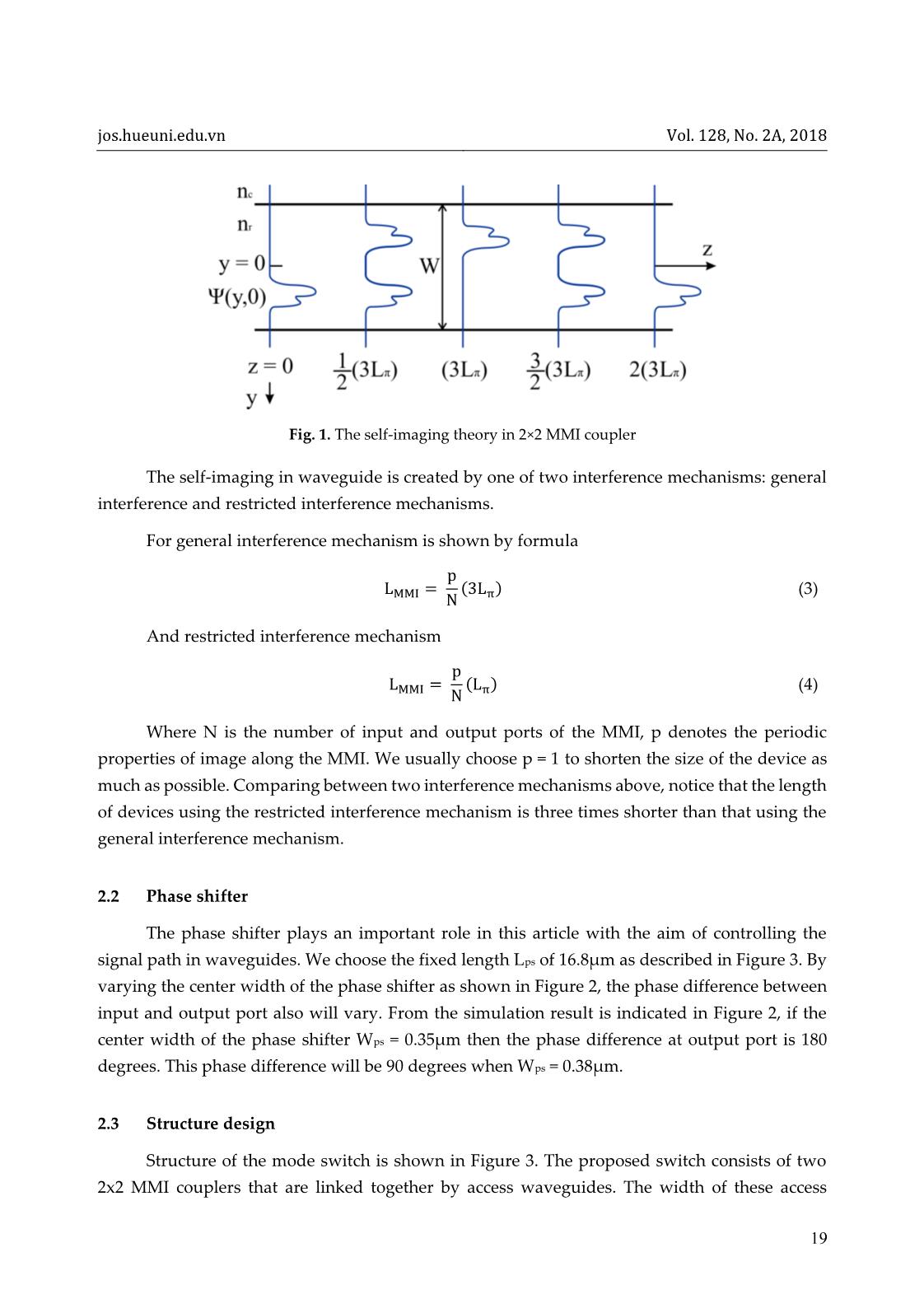
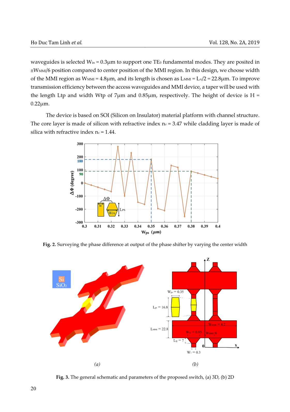
signal path in waveguides. We choose the fixed length Lps of 16.8μm as described in Figure 3. By
varying the center width of the phase shifter as shown in Figure 2, the phase difference between
input and output port also will vary. From the simulation result is indicated in Figure 2, if the
center width of the phase shifter Wps = 0.35μm then the phase difference at output port is 180
degrees. This phase difference will be 90 degrees when Wps = 0.38μm.
2.3 Structure design
Structure of the mode switch is shown in Figure 3. The proposed switch consists of two
2x2 MMI couplers that are linked together by access waveguides. The width of these access
Ho Duc Tam Linh et al. Vol. 128, No. 2A, 2019
20
waveguides is selected Win = 0.3μm to support one TE0 fundamental modes. They are posited in
±WMMI/6 position compared to center position of the MMI region. In this design, we choose width
of the MMI region as WMMI = 4.8μm, and its length is chosen as LMMI = Lπ/2 = 22.8μm. To improve
transmission efficiency between the access waveguides and MMI device, a taper will be used with
the length Ltp and width Wtp of 7μm and 0.85μm, respectively. The height of device is H =
0.22μm.
The device is based on SOI (Silicon on Insulator) material platform with channel structure.
The core layer is made of silicon with refractive index nr = 3.47 while cladding layer is made of
silica with refractive index nc = 1.44.
Fig. 2. Surveying the phase difference at output of the phase shifter by varying the center width
(a) (b)
Fig. 3. The general schematic and parameters of the proposed switch, (a) 3D, (b) 2D
jos.hueuni.edu.vn Vol. 128, No. 2A, 2018
21
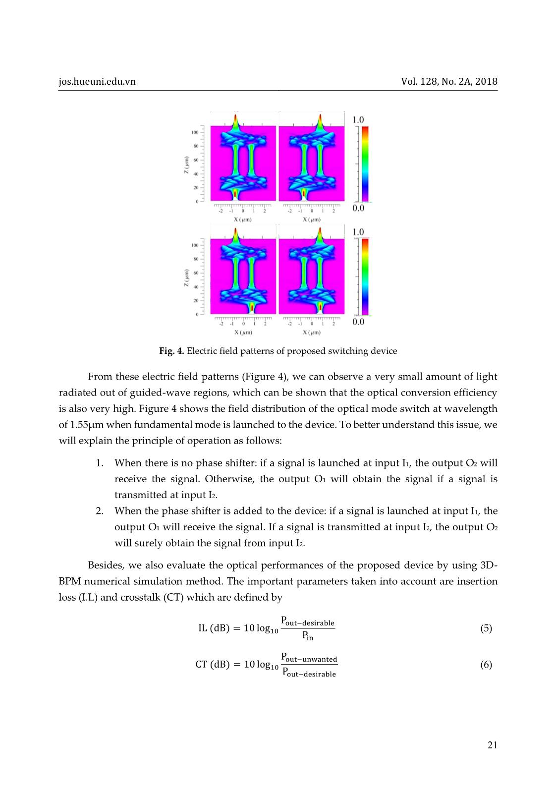
Fig. 4. Electric field patterns of proposed switching device
From these electric field patterns (Figure 4), we can observe a very small amount of light
radiated out of guided-wave regions, which can be shown that the optical conversion efficiency
is also very high. Figure 4 shows the field distribution of the optical mode switch at wavelength
of 1.55μm when fundamental mode is launched to the device. To better understand this issue, we
will explain the principle of operation as follows:
1. When there is no phase shifter: if a signal is launched at input I1, the output O2 will
receive the signal. Otherwise, the output O1 will obtain the signal if a signal is
transmitted at input I2.
2. When the phase shifter is added to the device: if a signal is launched at input I1, the
output O1 will receive the signal. If a signal is transmitted at input I2, the output O2
will surely obtain the signal from input I2.
Besides, we also evaluate the optical performances of the proposed device by using 3D-
BPM numerical simulation method. The important parameters taken into account are insertion
loss (I.L) and crosstalk (CT) which are defined by
IL (dB) = 10 log10
Pout−desirable
Pin
 (5)
CT (dB) = 10 log10
Pout−unwanted
Pout−desirable
 (6)
Ho Duc Tam Linh et al. Vol. 128, No. 2A, 2019
22
Where Pin is the input power of the device, Pout-desirable is the received power at the desired
output and Pout-unwanted is the leakage power at the another ouput.
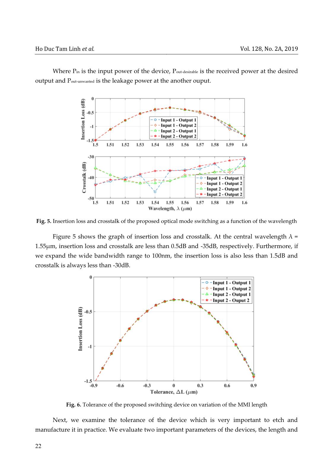
Fig. 5. Insertion loss and crosstalk of the proposed optical mode switching as a function of the wavelength
Figure 5 shows the graph of insertion loss and crosstalk. At the central wavelength λ =
1.55μm, insertion loss and crosstalk are less than 0.5dB and -35dB, respectively. Furthermore, if
we expand the wide bandwidth range to 100nm, the insertion loss is also less than 1.5dB and
crosstalk is always less than -30dB.
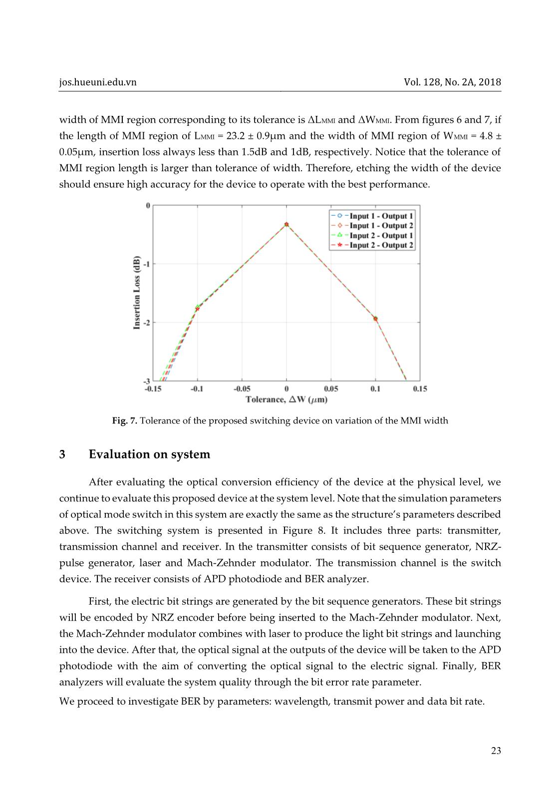
Fig. 6. Tolerance of the proposed switching device on variation of the MMI length
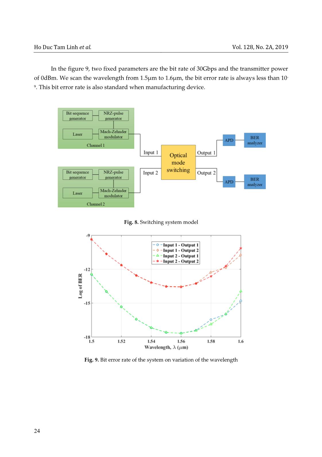
Next, we examine the tolerance of the device which is very important to etch and
manufacture it in practice. We evaluate two important parameters of the devices, the length and
jos.hueuni.edu.vn Vol. 128, No. 2A, 2018
23
width of MMI region corresponding to its tolerance is ΔLMMI and ΔWMMI. From figures 6 and 7, if
the length of MMI region of LMMI = 23.2 ± 0.9μm and the width of MMI region of WMMI = 4.8 ±
0.05μm, insertion loss always less than 1.5dB and 1dB, respectively. Notice that the tolerance of
MMI region length is larger than tolerance of width. Therefore, etching the width of the device
should ensure high accuracy for the device to operate with the best performance.
Fig. 7. Tolerance of the proposed switching device on variation of the MMI width
3 Evaluation on system
After evaluating the optical conversion efficiency of the device at the physical level, we
continue to evaluate this proposed device at the system level. Note that the simulation parameters
of optical mode switch in this system are exactly the same as the structure’s parameters described
above. The switching system is presented in Figure 8. It includes three parts: transmitter,
transmission channel and receiver. In the transmitter consists of bit sequence generator, NRZ-
pulse generator, laser and Mach-Zehnder modulator. The transmission channel is the switch
device. The receiver consists of APD photodiode and BER analyzer.
First, the electric bit strings are generated by the bit sequence generators. These bit strings
will be encoded by NRZ encoder before being inserted to the Mach-Zehnder modulator. Next,
the Mach-Zehnder modulator combines with laser to produce the light bit strings and launching
into the device. After that, the optical signal at the outputs of the device will be taken to the APD
photodiode with the aim of converting the optical signal to the electric signal. Finally, BER
analyzers will evaluate the system quality through the bit error rate parameter.
We proceed to investigate BER by parameters: wavelength, transmit power and data bit rate.
Ho Duc Tam Linh et al. Vol. 128, No. 2A, 2019
24
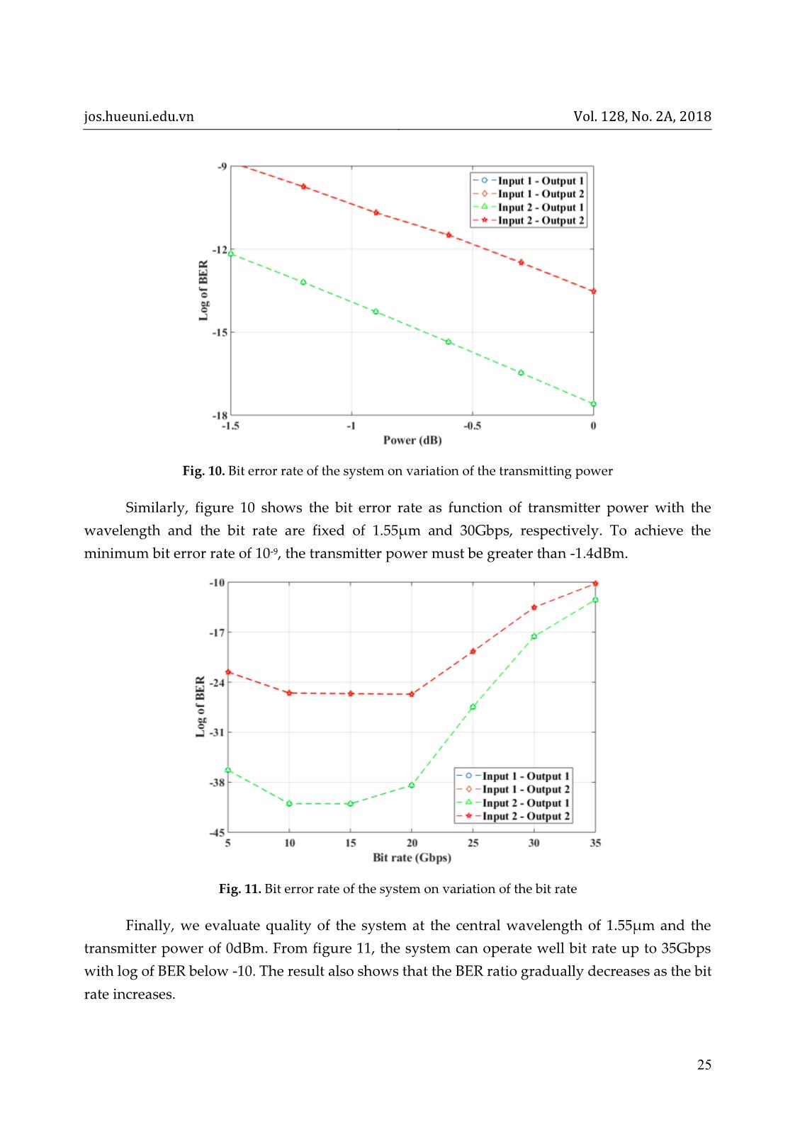
In the figure 9, two fixed parameters are the bit rate of 30Gbps and the transmitter power
of 0dBm. We scan the wavelength from 1.5μm to 1.6μm, the bit error rate is always less than 10-
9. This bit error rate is also standard when manufacturing device.
Fig. 8. Switching system model
Fig. 9. Bit error rate of the system on variation of the wavelength
jos.hueuni.edu.vn Vol. 128, No. 2A, 2018
25
Fig. 10. Bit error rate of the system on variation of the transmitting power
Similarly, figure 10 shows the bit error rate as function of transmitter power with the
wavelength and the bit rate are fixed of 1.55μm and 30Gbps, respectively. To achieve the
minimum bit error rate of 10-9, the transmitter power must be greater than -1.4dBm.
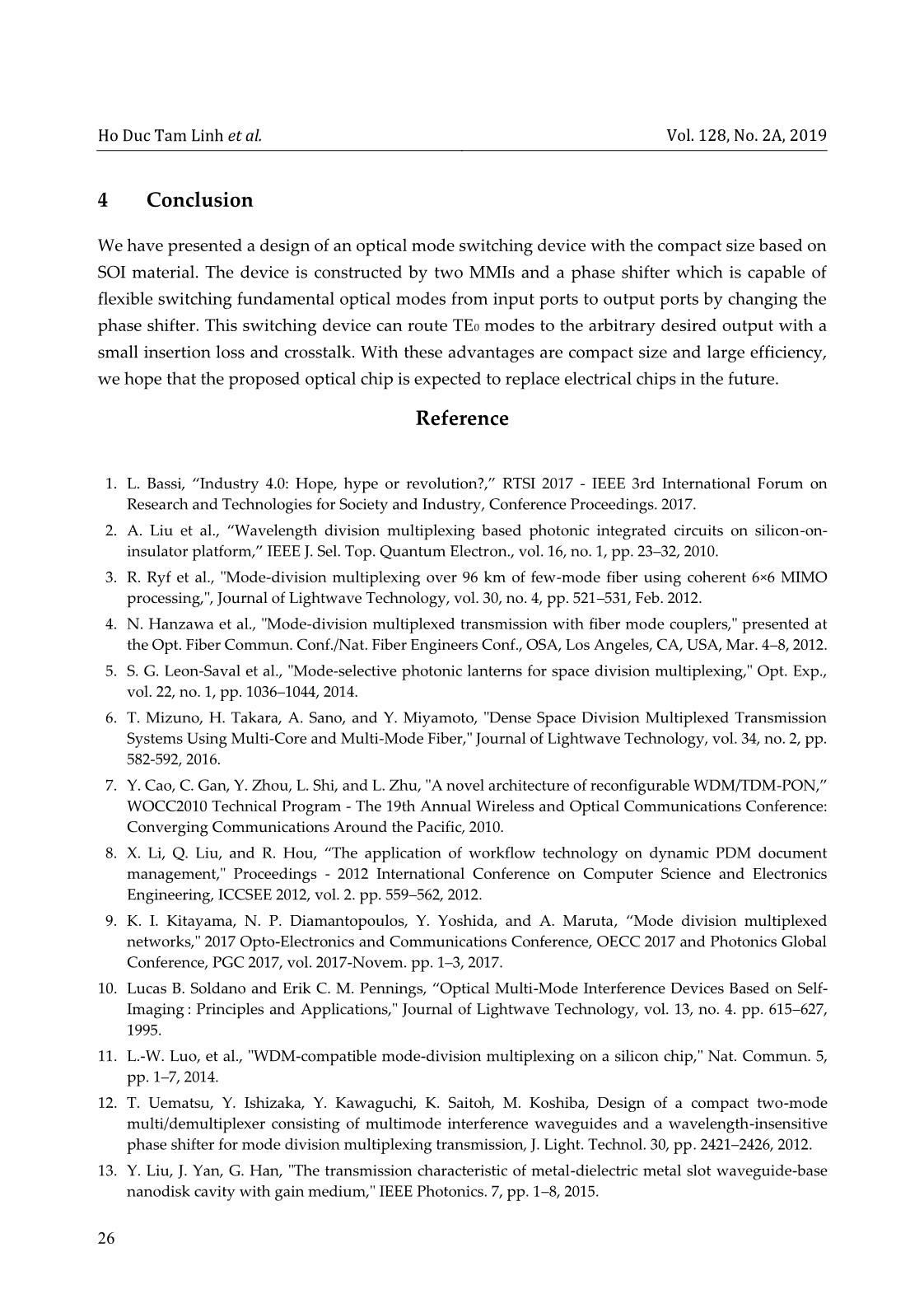
Fig. 11. Bit error rate of the system on variation of the bit rate
Finally, we evaluate quality of the system at the central wavelength of 1.55μm and the
transmitter power of 0dBm. From figure 11, the system can operate well bit rate up to 35Gbps
with log of BER below -10. The result also shows that the BER ratio gradually decreases as the bit
rate increases.
Ho Duc Tam Linh et al. Vol. 128, No. 2A, 2019
26
4 Conclusion
We have presented a design of an optical mode switching device with the compact size based on
SOI material. The device is constructed by two MMIs and a phase shifter which is capable of
flexible switching fundamental optical modes from input ports to output ports by changing the
phase shifter. This switching device can route TE0 modes to the arbitrary desired output with a
small insertion loss and crosstalk. With these advantages are compact size and large efficiency,
we hope that the proposed optical chip is expected to replace electrical chips in the future.
Reference
1. L. Bassi, “Industry 4.0: Hope, hype or revolution?,” RTSI 2017 - IEEE 3rd International Forum on
Research and Technologies for Society and Industry, Conference Proceedings. 2017.
2. A. Liu et al., “Wavelength division multiplexing based photonic integrated circuits on silicon-on-
insulator platform,” IEEE J. Sel. Top. Quantum Electron., vol. 16, no. 1, pp. 23–32, 2010.
3. R. Ryf et al., "Mode-division multiplexing over 96 km of few-mode fiber using coherent 6×6 MIMO
processing,", Journal of Lightwave Technology, vol. 30, no. 4, pp. 521–531, Feb. 2012.
4. N. Hanzawa et al., "Mode-division multiplexed transmission with fiber mode couplers," presented at
the Opt. Fiber Commun. Conf./Nat. Fiber Engineers Conf., OSA, Los Angeles, CA, USA, Mar. 4–8, 2012.
5. S. G. Leon-Saval et al., "Mode-selective photonic lanterns for space division multiplexing," Opt. Exp.,
vol. 22, no. 1, pp. 1036–1044, 2014.
6. T. Mizuno, H. Takara, A. Sano, and Y. Miyamoto, "Dense Space Division Multiplexed Transmission
Systems Using Multi-Core and Multi-Mode Fiber," Journal of Lightwave Technology, vol. 34, no. 2, pp.
582-592, 2016.
7. Y. Cao, C. Gan, Y. Zhou, L. Shi, and L. Zhu, "A novel architecture of reconfigurable WDM/TDM-PON,”
WOCC2010 Technical Program - The 19th Annual Wireless and Optical Communications Conference:
Converging Communications Around the Pacific, 2010.
8. X. Li, Q. Liu, and R. Hou, “The application of workflow technology on dynamic PDM document
management," Proceedings - 2012 International Conference on Computer Science and Electronics
Engineering, ICCSEE 2012, vol. 2. pp. 559–562, 2012.
9. K. I. Kitayama, N. P. Diamantopoulos, Y. Yoshida, and A. Maruta, “Mode division multiplexed
networks," 2017 Opto-Electronics and Communications Conference, OECC 2017 and Photonics Global
Conference, PGC 2017, vol. 2017-Novem. pp. 1–3, 2017.
10. Lucas B. Soldano and Erik C. M. Pennings, “Optical Multi-Mode Interference Devices Based on Self-
Imaging : Principles and Applications," Journal of Lightwave Technology, vol. 13, no. 4. pp. 615–627,
1995.
11. L.-W. Luo, et al., "WDM-compatible mode-division multiplexing on a silicon chip," Nat. Commun. 5,
pp. 1–7, 2014.
12. T. Uematsu, Y. Ishizaka, Y. Kawaguchi, K. Saitoh, M. Koshiba, Design of a compact two-mode
multi/demultiplexer consisting of multimode interference waveguides and a wavelength-insensitive
phase shifter for mode division multiplexing transmission, J. Light. Technol. 30, pp. 2421–2426, 2012.
13. Y. Liu, J. Yan, G. Han, "The transmission characteristic of metal-dielectric metal slot waveguide-base
nanodisk cavity with gain medium," IEEE Photonics. 7, pp. 1–8, 2015.
jos.hueuni.edu.vn Vol. 128, No. 2A, 2018
27
14. Y. Li, C. Li, C. Li, B. Cheng, C. Xue, "Compact two-mode (de)multiplexer based on symmetric y-junction
and multimode interference waveguides," Opt. Express 22, pp. 5781–5786, 2014.
15. D. Dang, B. Patra, R. Mahapatra, and M. Fiers, “Mode-Division-Multiplexed Photonic Router for High
Performance Network-on-Chip,” Proceedings of the IEEE International Conference on VLSI Design, vol.
2015-Febru, no. February. pp. 111–116, 2015.
16. H. K. T. Xinru Wu, Chaoran Huang, Ke Xu, Chester Shu, “Mode-Division Multiplexing for Silicon
Photonic Network-on-Chip.”, Journal of Lightwave Technology, pp. 3223–3228, 2017.
17. Y. Xiong, R. B. Priti, and O. Liboiron-Ladouceur, “High-speed two-mode switch for mode-division
multiplexing optical networks,” Optica, vol. 4, no. 9, p. 1098, 2017.
18. Q. Lai, W. Hunziker, and H. Melchior, “Low-power compact 2 × 2 thermooptic silica-on-silicon
waveguide switch with fast response,” IEEE Photonics Technology Letters, vol. 10, no. 5. pp. 681–683,
1998.
19. L. B. Soldano, E. C.M.Pennings, Optical multi-mode interference devices based on self-imaging:
Principles and applications, Journal of Lightwave Technology, 13, pp. 615–627, 1995.
File đính kèm:
 design_a_2x2_compact_mode_switching_using_multimode_interfer.pdf

